Page 2 of 4
Re: Sketches please: a fewest-chips logic-only 816 system
Posted: Sat Sep 19, 2020 1:32 pm
by BillO
Out of reset, you need ROM at the top of Bank 0 to provide a vector and a handler routine. That's no different from a 6502. So that doesn't seem to work if you're only decoding with A22/23, since you have all RAM in Bank 0, and the ROM is all in high banks.
You're right! I should read the spec sheet once in a while, eh?
Re: Sketches please: a fewest-chips logic-only 816 system
Posted: Sat Sep 19, 2020 1:36 pm
by BillO
Nice!
Just one thought though, is it really a computer if it has no I/O?
Just throw in one more chip, call it 11 and have something that is useful, maybe?
Re: Sketches please: a fewest-chips logic-only 816 system
Posted: Sat Sep 19, 2020 2:47 pm
by GARTHWILSON
Just one thought though, is it really a computer if it has no I/O?
I once had a boss who wanted to save money and prune things unreasonably, so we joked that we could eliminate the I/O, and that it would have the benefit and cost savings that without I/O, the customer would never notice any bugs.
Re: Sketches please: a fewest-chips logic-only 816 system
Posted: Sat Sep 19, 2020 4:10 pm
by BillO
Just one thought though, is it really a computer if it has no I/O?
I once had a boss who wanted to save money and prune things unreasonably, so we joked that we could eliminate the I/O, and that it would have the benefit and cost savings that without I/O, the customer would never notice any bugs.
LOL!
That would definitely cut down on the support calls ...
Re: Sketches please: a fewest-chips logic-only 816 system
Posted: Sat Sep 19, 2020 5:06 pm
by Dr Jefyll
LOL!
That would definitely cut down on the support calls ...
Yup -- it breaks the cycle in TWO places!

No way for garbage to go in, and no way for garbage to get out!

Re: Sketches please: a fewest-chips logic-only 816 system
Posted: Sat Sep 19, 2020 5:28 pm
by BigEd
I can't resist mentioning
H G Muller's 'matchbox' chess computer, battery powered, '816 based, no ROM, fits in a matchbox and plays chess:
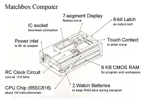
It looks pretty minimal. I think the program is downloaded into RAM using a ROM in the socket, then retained on battery power.
Re: Sketches please: a fewest-chips logic-only 816 system
Posted: Sat Sep 19, 2020 6:18 pm
by Chromatix
If we discard the handling of VDA, VPA [...]
Sounds to me like a reasonable option, given that many I/O devices have no need for protection against spurious reads.
Of course the 6522 and 6551 are notable exceptions (and popular choices for 65xx systems), but their protection requires zero gates. Assuming the active-
high Chip Select input is otherwise unused, it can simply be connected to VDA. (VPA can be ignored... unless you intend to execute I/O device's content as if it were code!)
The 28L92 would also be a good choice for an '816 based system, but it doesn't have the additional active-high select input, and I think I recall seeing in other threads that it can definitely be sensitive to spurious accesses. One solution is to only access it using instructions that have no dead cycles, which I think includes all the long addressing modes (since the carry cycles for indexing are absorbed by loading the high byte of the address). Another side benefit of mapping I/O high!
With six selectors on the '138 available for I/O (four if we reserve two of them to provide a contiguous RAM area), there is no problem whatsoever attaching, say, a 28L92 UART, a DS1511 RTC, a VIA for a local keymatrix and bit-banged SPI to a display, and still have space for additional devices without need for further decoding. Space for all these could be provided on a PCB, and the builder could assemble them in any desired order after the core.
Re: Sketches please: a fewest-chips logic-only 816 system
Posted: Sat Sep 19, 2020 11:45 pm
by jds
Probably not in the spirit of this challenge, but I think I can reduce the chips quite a bit by making use of a 6530-004 TIM chip, this provides ROM and I/O in one package. The I/O (and here is the cheating) could be used for bank select outputs for the RAM, therefore eliminating the need for the latch on the high address bits, at the expense of eliminating many of the advantages of the 816.
The ROM should work well enough in emulation mode, and provides additional useful features such as a 300 bps serial console port.
I don’t think this would be a very usable system, but it could result in a working 65816 with as few as 5 chips.
Re: Sketches please: a fewest-chips logic-only 816 system
Posted: Sun Sep 20, 2020 12:06 am
by Chromatix
While sketching out the details, I found that the 28L92 has an active-high reset line, opposite to anything else in the system. As a workaround without using any extra chips, I'm wiring it up to an output on the VIA.
Meanwhile, the VIA also serves as a Mode 3 SPI master, which can be used to drive a write-only display such as the Sharp Memory LCD. It should also be straightforward to attach a keymatrix to the VIA, allowing for local input and display rather than always going through the UART.
Re: Sketches please: a fewest-chips logic-only 816 system
Posted: Sun Sep 20, 2020 11:43 am
by BigEd
> therefore eliminating the need for the latch on the high address bits, at the expense of eliminating many of the advantages of the 816
Subversive!
Re: Sketches please: a fewest-chips logic-only 816 system
Posted: Sun Sep 20, 2020 1:21 pm
by Chromatix
Okay, here's what I've worked out thus far. First, the basic core:
Then the peripheral devices; you can probably start with just the VIA, and add the others around it. I've left most of the external connections to the VIA and UART as exercises for the reader:
And finally, the extra memory chips to give a 1MB contiguous RAM area:
All of this relies on just two 74HC-series chips for glue logic, and one more as a bank address latch.
Re: Sketches please: a fewest-chips logic-only 816 system
Posted: Sun Sep 20, 2020 7:41 pm
by BigDumbDinosaur
Okay, here's what I've worked out thus far. First, the basic core...All of this relies on just two 74HC-series chips for glue logic, and one more as a bank address latch.
74HC likely won't be fast enough for latching the bank logic.
Re: Sketches please: a fewest-chips logic-only 816 system
Posted: Sun Sep 20, 2020 7:48 pm
by Chromatix
You my notice that the positive Phi2 (to the CPU) is actually delayed by one 74HC gate relative to the inverted /Phi2 sent to the latch, rather than the other way round. So as long as the clock speed is modest (as it has to be anyway with a slow EEPROM and no wait-states), 74HC *is* fast enough.
Re: Sketches please: a fewest-chips logic-only 816 system
Posted: Tue Sep 22, 2020 4:46 am
by Michael
Sorry late to the party, guys and gals.
I have an idea though several details are yet to be worked out. How about using simple I/O address decode logic and selecting both RAM and ROM for memory operations but directing the /RD signal to only one or the other? The idea here is that a switch is set at power-up (reset) to select ROM 'read' and RAM 'write' in order to copy a ROM image into RAM, then the switch is toggled to select RAM 'read' and RAM 'write' effectively mapping ROM out of the address space. With the simple address decoding in the example drawing below, there will be four 32K ROM images spanning the 128K address space when ROM 'read' is enabled.
Another switch might be used to map an I/O block into or out of the address space. Again, the simple address decoding would place the I/O block into each 64K 'bank' but when the I/O block is turned off you have contiguous RAM memory. The example below should scale up to a 256K or 512K RAM chip, as well as a larger ROM or FLASH chip.
I'm not familiar with 65C816 and what it takes to qualify RAM 'read' or 'write' operations. I'm also not exactly sure how to take advantage of the high order address lines (A21..A23) as potential triggers or inputs for the <Read> and <I/O> switches.
Stay safe. Cheerful regards, Mike, K8LH
Re: Sketches please: a fewest-chips logic-only 816 system
Posted: Tue Sep 22, 2020 7:25 am
by Chromatix
At the basic level, you can interface the '816 like a 6502, relying on just Phi2 and R/W as control signals. The wrinkles are that A16-23 (the bank address) are multiplexed onto D0-7, so you have to latch them during Phi1 in order to make use of them during Phi2, and that VDA and VPA indicate Valid Data Address and Valid Program Address respectively; if both are high simultaneously, that's a replacement for the SYNC signal. In short, if VDA and VPA are both low then it is desirable to deselect all devices, as it's an internal-operation cycle. Finally, if RDY is low (typically due to wait states) then the bank address must not be latched because the data bus remains in data mode.
All of this is handled appropriately by the circuits I've posted, which you may want to review. With two glue-logic chips and an octal latch, you can have a minimal interface and address decoding which assumes that there are no wait-states (and does not provide any), and does not fully handle VDA and VPA (so every memory cycle is assumed to be valid, except that the VIA is qualified by VDA). With four glue-logic chips and an octal latch, you can have full handling of VDA, VPA and RDY, together with a trick that maps out the ROM when the CPU leaves Emulation mode for Native mode (using the fact that the '816 conveniently presents the E, M and X flag bits on output pins).