Page 2 of 4

Re: Experimental TTL implementation of the 6522

Posted: Mon Mar 04, 2019 8:39 pm
by Chromatix
A nitpick: I'm not sure the VIC-II's extra accesses ever appeared on the 6502 bus itself, because the VIC-II was also the DRAM controller and had direct access to it. The 6502 was only halted occasionally because the VIC-II couldn't service CPU requests at times of peak display bandwidth requirements.

Re: Experimental TTL implementation of the 6522

Posted: Tue Mar 05, 2019 2:08 pm
by BigEd
Wow ttlworks, what dedication, and what a creation. Needing 8 boards to re-implement really reminds us of how many transistors could be in even a commodity chip from back in the day.

Re: Experimental TTL implementation of the 6522

Posted: Tue Mar 05, 2019 3:29 pm
by Martin_H
It is a thing of beauty. It also makes me appreciate the 6522!

Re: Experimental TTL implementation of the 6522

Posted: Wed Mar 06, 2019 12:56 pm
by Drass
So much knowledge and inspiration here. Just beautiful! Thank you for blazing the trail ttlworks!

Re: Experimental TTL implementation of the 6522

Posted: Wed Mar 06, 2019 9:45 pm
by daniMolina
I can't even start to explain how awesome is to see this, thank you so much for sharing all this information.

For those of you who don't know it, I'm the guy with the crazy idea of reimplementing the 6526 just because.... well... I just want to have some fun :)

I'm running some concept tests at the moment... because I'm a total noob I'm afraid. If I get any result, other than blowing up my C64, I'll start a thread on this to share my progress.

Again, thanks, I can't say it enough times!

Re: Experimental TTL implementation of the 6522

Posted: Wed Mar 06, 2019 11:58 pm
by White Flame
Chromatix wrote:
A nitpick: I'm not sure the VIC-II's extra accesses ever appeared on the 6502 bus itself, because the VIC-II was also the DRAM controller and had direct access to it. The 6502 was only halted occasionally because the VIC-II couldn't service CPU requests at times of peak display bandwidth requirements.
The VIC-II has DRAM refresh in it, but the CPU doesn't talk "through" the VIC-II as in modern "memory controller"s. There's only 1 bus to the main RAM, and both CPU/VIC-II drive it in alternating phases, meaning it effectively timeslices 2MHz accesses, each chip hitting it at 1MHz each.

Sometimes the VIC-II needed more memory access cycles than just its half, so it halted the 6510 to use full 2MHz access to get those things done in time. This is usually every 8 rasterlines to pull in 40 screen bytes, or a few bytes every line if lots of sprites were active during them.

The VIC-II however did have its own dedicated bus to the 1Kx4 color memory chip, so it effectively could do combined 12-bit wide data accesses during its ownership of the main 8-bit data bus. That might be what you're remembering.

--

More on topic, neat! :)

Re: Experimental TTL implementation of the 6522

Posted: Thu Mar 07, 2019 4:12 pm
by ttlworks
Thanks for the kind words and the appreciation.

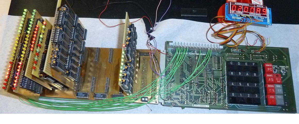
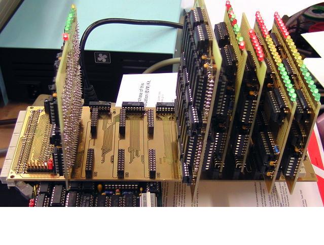
I also had an experimental 6521\6821 TTL implementation,
the experimental 6545\6845 TTL implementation had some serious issues (but at least it had generated a picture),
and the experimental 6551\6850 TTL implementation had failed (having three different clock domains in one design wasn't fun).

Hey, you recognize the pioneer by the arrows in his back. :)

;---

But back on topic:

The problem with the C64 timing is, that the 6510 address\data pins are in high impedance during PHI2 = LOW,
and that it takes some time until the 6510 puts the address on the bus after the rising edge of PHI2.

When taking a closer look at the bus timing in the 6526 and NMOS 6522 datasheets,
it appears that the 6526 needs a stable address on the bus before the falling edge of PHI2,
but the 6522 needs a stable address on the bus before the rising edge of PHI2.

So when looking into old schematics which show a 6522 on the C64 expansion port,
I think it isn't unusual to see something like PHI2 delayed with two flipflops clocked by the dot clock
for generating PHI2' for the 6522.

For building a 6526 TTL implementation, the TTL 6522 only might be "half of the rent", of course,
because in the 6526 a few things are quite different.

I see two main problems when trying to build a 20MHz TTL 6526:
First, the two 16 Bit timers could be "chained", so we need to keep an eye on that propagation delay for the TTL counters.
Second, that odd BCD clock... counter propagation delay might be getting an issue there, too.

Re: Experimental TTL implementation of the 6522

Posted: Mon Mar 25, 2019 4:59 pm
by ttlworks
Since I don't know, for how long I'll be able to open Eagle 3.55 project files,
I think it's a good idea to post the rest of it... as spare time permits this.

;---

X23 was sort of an "experimental 6523", which had three I\O ports.

The X23 backplane was plugged on top of the 2B22 bus interface from the X22 TTL 6522 project,
jumper settings on the 2B22 bus interface just were different from "X22 mode", of course.

For the I\O ports, 1PA22 and 1PB22 modules from the X22 project were used too.
BTW: pinout for 1PA22 (open collector outputs) and 1PB22 (push/pull outputs) modules were identical.

Image

It was my test adaptor for the 2B22 bus interface and the 1PA22\1PB22 I\O modules,
because it took less current from the power supply than X22 when running loop_back tests
with a ribbon cable between two I\O modules.

Oh, and I forgot to mention:
IIRC the I\O connectors on the X22, X21 and X23 backplanes were supposed to be compatible to Daryl Rictor's SBC2.
x23_1.png
x23_2.png
x23_3.png

Re: Experimental TTL implementation of the 6522

Posted: Mon Mar 25, 2019 5:12 pm
by ttlworks
X21 was an experimental 6521\6821 implementation.
From the datasheets, I failed to see a noticable difference between NMOS 6521 and 6821.

Image

2B22 bus interface from the X22 project (6522) is plugged into the 6502 computer.
X21 backplane is plugged into the 2B22 bus interface (which has different jumper settings from "6522 mode" and "6523 mode", of course).

Plugged into the X21 backplane, we have:
1* 1PA22, Port A module
1* 1PB22, Port B module
2* H21, handshake module

Re: Experimental TTL implementation of the 6522

Posted: Mon Mar 25, 2019 5:18 pm
by ttlworks
We got 2B22, 1PA22, 1PB22 already covered up in the thread.

So I'm posting the X21 backplane:

Image
x21_1.png
x21_2.png
x21_3.png

Re: Experimental TTL implementation of the 6522

Posted: Mon Mar 25, 2019 5:23 pm
by ttlworks
H21 was the handshake module, two modules required.
The H21 handshake modules also had contained the interrupt logic.

Image
h21_1.png
h21_2.png
h21_3.png
H21_4.png
h21_5.png
h21_6.png
h21_7.png

Re: Experimental TTL implementation of the 6522

Posted: Mon Mar 25, 2019 5:28 pm
by ttlworks
Now for another untested paper design,
an experimental TTL 6521 which is supposed to be able to make 20MHz.

You better carefully check and re_think everything before trying to build something based on these old schematics.
6521_1.png
6521_2.png
...And that's enough for a day. 6532 will be next.

Re: Experimental TTL implementation of the 6522

Posted: Mon Mar 25, 2019 5:29 pm
by BigEd
Thanks for posting your projects!

Re: Experimental TTL implementation of the 6522

Posted: Mon Mar 25, 2019 6:38 pm
by GARTHWILSON
Eye candy!

Re: Experimental TTL implementation of the 6522

Posted: Sat Apr 06, 2019 12:07 pm
by ttlworks
Thanks for the kind words.

Image

Right: 1980, my first hobby computing project. Elektor Junior Computer hobby kit.
Left: 2015, my last hobby computing project. X32, experimental TTL implementation of the 6532.

X32 had some bugs, be warned.

Plugged into the X32 backplane, we are supposed to have:
1* 1PA22, Port A module
1* 1PB22, Port B module
1* T32, timer module
1* I32, timer control and interrupt module
4* R32, 4* 32 Bytes of RAM that is... (only 1 module was built)
1* B32, bus interface

Image