Page 2 of 9
Re: Writing in EEPROM and reading by 6502
Posted: Fri Dec 07, 2018 2:08 am
by hitlp
Hello guys.
The question of memory address became much clearer. But now I'm stuck at another point. I picked up my logic analyzer (8 channels) and plugged it into the ROM data bus (D0-D7).
My ROM is as follows:
0x0000 A9 (LDA)
0x0001 12 (# $ 12)
0x0002 4C (JMP)
0x0003 00
0x0004 80 (here it comes back from the 0x00)
....
0x077A 00 (NMI lo)
0x077B 80 (NMI hi)
0x077C 00 (RESET lo)
0x077D 80 (RESET hi)
0x077E 00 (IRQ)
0x077F 80 (IRQ hi)
Looking at the logic analyzer, let's say this is the time moment "t":
If you look at the bus, it will:
80 (NMI hi)
00 (reset lo)
80 (reset hi)
00 (irq lo)
80 (irq hi)
A9 (lda)
12 ($12)
4C (loop)
00
80
So far I believe that everything is ok. At time "t + 1" time, it executes everything again, passing through the vectors. Should not it after the loop (8000) go back to the A9?
I do not know if my explanation was clear .. thanks!
Re: Writing in EEPROM and reading by 6502
Posted: Fri Dec 07, 2018 2:42 am
by Chromatix
The "00 80" at the end of your trace is the address operand of the JMP (4C) instruction, not from the vector table. The cycle immediately following that *should* be the LDA fetch from address $8000.
You should therefore have a repeating pattern of 5 cycles (2 for LDA immediate, 3 for JMP absolute), on both the data and address lines. If you don't, you might be mishandling the IRQ or NMI signals, for example.
Re: Writing in EEPROM and reading by 6502
Posted: Fri Dec 07, 2018 4:18 am
by Dr Jefyll
The "00 80" at the end of your trace is the address operand of the JMP (4C) instruction, not from the vector table. The cycle immediately following that *should* be the LDA fetch from address $8000.
Chromatix is right. The cycle immediately following $4C $00 $80 *should* be the $A9 (the LDA opcode that's at $8000).
Instead what got fetched is $00, which is a BRK instruction. (That explains why another vector was subsequently fetched. BRK is a software interrupt.)
But why did $00 get fetched? I believe it's because the fetch WASN'T from $8000, and that's because the JMP never happened.
One possible explanation is that $4C (the JMP opcode you intended) is
not what the CPU saw, even though that's what the *ROM* contains. This can result from a wiring error, such as when some of the data bus lines get transposed between the ROM and the CPU. This will distort $4C (at the ROM) into something else at the processor. Please carefully check your wiring -- D0 to D0, D1 to D1 and so on.
(BTW, you're welcome to include images as attachments to your post. It's not necessary to use Imgur.)
Re: Writing in EEPROM and reading by 6502
Posted: Fri Dec 07, 2018 4:37 am
by GARTHWILSON
Is this:
Code: Select all
0x077A 00 (NMI lo)
0x077B 80 (NMI hi)
0x077C 00 (RESET lo)
0x077D 80 (RESET hi)
0x077E 00 (IRQ)
0x077F 80 (IRQ hi)
just a typing error? The vectors should be at $7FFA to $7FFF of the 32KB ROM, not $77A to $77F. And if the processor is cycling through them, if it lands such that it's just seeing 80 00, that's BRA (Branch Relative Always, or BRanch Always) 00 which means it's not affecting the program counter any, so it just goes on the the next address. The reset sequence is six cycles long. This should be the first thing you see when execution starts. The NMI and IRQ sequences are seven cycles long.
Re: Writing in EEPROM and reading by 6502
Posted: Fri Dec 07, 2018 12:27 pm
by hitlp
The "00 80" at the end of your trace is the address operand of the JMP (4C) instruction, not from the vector table. The cycle immediately following that *should* be the LDA fetch from address $8000.
Chromatix is right. The cycle immediately following $4C $00 $80 *should* be the $A9 (the LDA opcode that's at $8000).
Instead what got fetched is $00, which is a BRK instruction. (That explains why another vector was subsequently fetched. BRK is a software interrupt.)
But why did $00 get fetched? I believe it's because the fetch WASN'T from $8000, and that's because the JMP never happened.
One possible explanation is that $4C (the JMP opcode you intended) is
not what the CPU saw, even though that's what the *ROM* contains. This can result from a wiring error, such as when some of the data bus lines get transposed between the ROM and the CPU. This will distort $4C (at the ROM) into something else at the processor. Please carefully check your wiring -- D0 to D0, D1 to D1 and so on.
(BTW, you're welcome to include images as attachments to your post. It's not necessary to use Imgur.)
Yes. I had imagined that a BRK was happening but I have no idea why. I will double-check the connection between the CPU and the ROM.
Re: Writing in EEPROM and reading by 6502
Posted: Fri Dec 07, 2018 12:30 pm
by hitlp
Is this:
Code: Select all
0x077A 00 (NMI lo)
0x077B 80 (NMI hi)
0x077C 00 (RESET lo)
0x077D 80 (RESET hi)
0x077E 00 (IRQ)
0x077F 80 (IRQ hi)
just a typing error? The vectors should be at $7FFA to $7FFF of the 32KB ROM, not $77A to $77F. And if the processor is cycling through them, if it lands such that it's just seeing 80 00, that's BRA (Branch Relative Always, or BRanch Always) 00 which means it's not affecting the program counter any, so it just goes on the the next address. The reset sequence is six cycles long. This should be the first thing you see when execution starts. The NMI and IRQ sequences are seven cycles long.
Hi GARTHWILSON,
Yes. Sorry. It was a typing error. The correct is:
Code: Select all
0x7FFA 00 (NMI lo)
0x7FFB 80 (NMI hi)
0x7FFC 00 (RESET lo)
0x7FFD 80 (RESET hi)
0x7FFE 00 (IRQ)
0x7FFF 80 (IRQ hi)
Re: Writing in EEPROM and reading by 6502
Posted: Sun Dec 09, 2018 2:57 am
by hitlp
Hey Guys.
I checked and checked again but apparently the wiring is correct. I had a question: could the 6502AP CPU be used with a clock equal to 1 MHz?
By manual the 6502AP is compatible with 2 MHz. Could this underclock affect the operation?
Re: Writing in EEPROM and reading by 6502
Posted: Sun Dec 09, 2018 3:02 am
by GARTHWILSON
The NMOS 6502's minimum clock rate is specified to be 100kHz. It will usually successfully run down at half of that—it's just that it's not guaranteed to. Anyway, 1MHz on a 2MHz part is no problem.
Re: Writing in EEPROM and reading by 6502
Posted: Sun Dec 09, 2018 4:47 am
by Dr Jefyll
I checked and checked again but apparently the wiring is correct.
Hmmm. You haven't yet shared the schematic with us, nor any photos. But if you'd rather figure things out on your own that's OK; we'll stop trying to
guess what's wrong.
Here is a link describing the NOP Generator I mentioned earlier. You don't have to build one; if you wish you can do the test using your EEPROM instead, as I
explained.
The resulting behavior is the same. A0 should invert once every 2 Phi2 cycles; A1 inverts every 4 cycles; A2 inverts every 8 cycles, and so on.
-- Jeff
Re: Writing in EEPROM and reading by 6502
Posted: Sun Dec 09, 2018 9:24 am
by BigEd
Instead of dedicating all 8 channels of your logic analyser to the databus, consider swapping in the SYNC signal for one of them. You should still be able to follow along - if it's too hard, then take multiple traces, one with D7 swapped out, one with D0, and you should be able to line the two traces up.
Re: Writing in EEPROM and reading by 6502
Posted: Mon Dec 10, 2018 12:59 pm
by hitlp
I checked and checked again but apparently the wiring is correct.
Hmmm. You haven't yet shared the schematic with us, nor any photos. But if you'd rather figure things out on your own that's OK; we'll stop trying to
guess what's wrong.
Here is a link describing the NOP Generator I mentioned earlier. You don't have to build one; if you wish you can do the test using your EEPROM instead, as I
explained.
The resulting behavior is the same. A0 should invert once every 2 Phi2 cycles; A1 inverts every 4 cycles; A2 inverts every 8 cycles, and so on.
-- Jeff
Hello Dr. Jefyll,
I'm sorry for not putting the schematic before. Attached I put as is the CPU with the ROM to test the code already quoted. Does it have something wrong ??
Tonight, I'll try to test with the NOP instruction. I will put the results here.
Re: Writing in EEPROM and reading by 6502
Posted: Mon Dec 10, 2018 2:44 pm
by Dr Jefyll
Does it have something wrong ??
No, it's OK... for the very simple tests you're doing, at least. And you said /OE and /CE are tied low, and /WE is tied high. (In a more typical setting this will not be satisfactory.) I did want to double check what you're doing, though. When assisting newcomers, we on the forum are constantly on the lookout for things that have been misunderstood or overlooked.
Tonight, I'll try to test with the NOP instruction. I will put the results here.
Sounds good. Have fun, and keep us posted!

-- Jeff
Re: Writing in EEPROM and reading by 6502
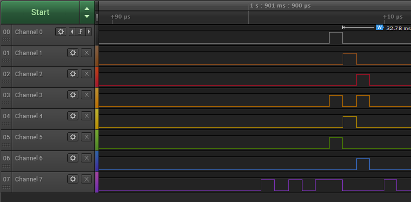
Posted: Sat Dec 15, 2018 3:09 am
by hitlp
Hello guys
Make the data bus for expert 11101010 (EA) which corresponds to the NOP instruction. The image represents the address bar reading from A0 - A7.
Question: Does NOP run clock cycles? In my case, he is using only one. The frequency of the bus is:
CPU CLK = 1 MHz
A0 = 500 KHz.
A1 = 250 KHz
A2 = 125 KHz
A3 = 62.5 KHz
A4 = 31.21 KHz
A5 = 15.61 KHz
A6 = 7.81 KHz
A7 = 3.9 KHz
Is that correct? Thank you.
Re: Writing in EEPROM and reading by 6502
Posted: Sat Dec 15, 2018 3:25 am
by GARTHWILSON
Question: Does NOP run clock cycles? In my case, he is using only one. The frequency of the bus is:
CPU CLK = 1 MHz
A0 = 500 KHz
[...]
Is that correct? Thank you.
Yes, that is correct. NOP is one byte but takes two cycles, which is why you see 500kHz on A0 instead of 1MHz. At 1MHz, a cycle is 1µs, not 2. [
Edit: I wrote too hastily.

At 1MHz clock rate, A0 will
change 500,000 times per second, not
cycle at 500,000 cycles per second.]
Re: Writing in EEPROM and reading by 6502
Posted: Sat Dec 15, 2018 3:29 am
by Chromatix
NOP ($EA) should take 2 cycles on any genuine 65xx family CPU. The first cycle reads the NOP opcode with SYNC high, the second cycle is a dummy read of the *next* byte with SYNC low.
Also note that a counter's least significant bit cycles at half the frequency of its trigger clock. It's very common to use counters as frequency dividers for that reason.
So with a 1MHz clock, SYNC should cycle at 500kHz, A0 should cycle at 250kHz, etc. If A0 is cycling at 500kHz, then something is wrong; the CPU is seeing a different opcode than the one ostensibly stored in your ROM.