After an internet search, to me it looks like there is no 65816 in VHDL yet. //November 2016.
Let's just hope, that the community does a VHDL 65816 before our only source for 65816 chips might run dry "by accident" someday.

Ok, for our 65C816 versus 68000 discussion we had "availability of chips",
and "VHDL cores as a replacement if chips won't be available anymore".
Another interesting topic would be software.
For 68k without MMU, there seem to be operating system kernals, but not so for the 65816.
;---
Another point is, that from the hardware point of view it feels like there is no "standard" when it comes
to 65816 hobby computer projects.
68K at least had the
VME bus which was designed with the 68000 DIP package pinout in mind.
While 80x86 certainly wasn't the most beautiful architecture around (sorry for even mentioning 80x86),
it looks like having a standard there (IBM PC, DOS,
ISA bus) made it a success.
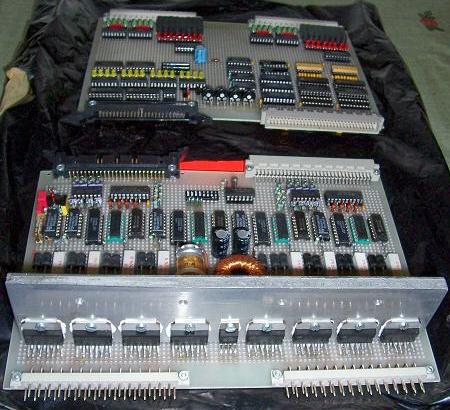
Its an interesting point that there are no 65816 cores available. But there are numerous examples of 65xx cores that have been extended. I don´t know why WDC doesn´t sell their 65C816 core as IP since the 65C02 has been available for long.
Anyway, I think I will stick to the 6502 and build on that. Its an interesting core since its so small, and one can fit several cores into a single CPLD. The 65816 is basically a 6502 with 16 bit addressing, which shouldn´t bee too difficult to extend (if anyone has the time).
Personally I am more interested in the 6502 and 6509 since an extension of the 6502 to increase address size WITHOUT increasing code size is profoundly more interesting in the long run. Why you ask? Well, I remember when my old workplace made the transition from an IBM System/36 to an IBM AS/400 in which all our code suddenly tripled in size. What a waste!
So I think having 8-bit instruction set with the ability to extend it within an FPGA (to 16/24/32 bits addressing) on a need-to-use basis with CISC-like translations. I think that is more forward thinking with respect of getting more computing power per watt.
What I hope to test (my long-term-plan):
Dual 6502 with pipelined in/out buffer and 32-bit databus. Basically run two instructions in paralell, but in a way that translates the instructions to a CISC. For example:
Which is four bytes that can be read on first cycle. 6502no1 handles LDA and 6502no2 handles STA (with update of register from 6502no1). So value #32 is stored into $02 on the second cycle.
For longer instructions, more data is needed, so a cache would be put up in order to read
on one cycle (which is 6 bytes). One could probably extend the databus to 48 or 64 bits (and more processor cores), but CISC like translations are the way to go to speed things up. So for example:
Code: Select all
LDX #$80
loop:
STX $A002,X
DEX
BNE loop
Is recognized as a loop and handled by the two cores with STA in one and DEX in the other, then some logic to keep them in the cores until the branch exits the loop. The output buffer would mean that write only happens when 32 bits can be written (in the case of 32-bit databus).
There are other more complex ways of handling this as well, but I have to start somewere. Currently I have connected a Lattice MACHXO3 to a Vic-20 through some voltage translators, but time has limited progress in the last weeks. I am probably starting with Arlets core as its small (and tags along 45MHz). The WDC core is 2.5 times larger(!) and ran at 75MHz, but its not free..
So what do you think?