Page 2 of 3
Re: OT: stacked (DIP) chips
Posted: Wed Sep 05, 2018 9:56 pm
by whartung
What would be awesome is if someone made a complete SBC (without the board) using nothing but stacked IC's.
And no micro-contollers or PLD's.

What's funny is that there's a book with, like, 7 different radio circuits or something. It's a book about making radios.
And I guess it was a review of the book where the person basically said that he wired the circuits together, and I think he just said something like "in the air".
Meaning, he used no board whatsoever, he simply tied the discrete components together, perhaps using hook up wire, and fired them up. Just a heap of components on his table, ensuring there were no accidental shorts.
There was a certain bit of elegance to that process.
Yes, here it is -- check out the pictures at the end of the review.
https://www.amazon.com/gp/customer-revi ... 0071799702
Re: OT: stacked (DIP) chips
Posted: Thu Jun 04, 2020 10:55 pm
by RalfK
May I add a design which I developed with a friend in the late 1980s?
The Macs were very expensive at this time in West-Germany. We bought some second hand Mac 512. But we wanted to have more RAM and SCSI means we really wanted to get a full equipped Mac Plus. Megabit DRAMs were very expensive at this time. So we decided to use 256kbit-DRAMs. The Mac board has installed 16 of these 41256. We added 112 to get full 4MB. But there is no space in a Mac. In theory
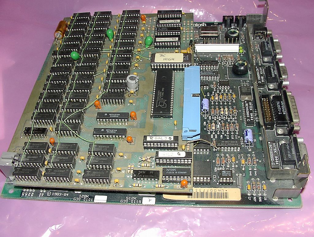
We ordered 10 PCBs and started to populate them for our Macs and the Macs of some friends. Some Macs were equipped with 2MB, most of them with 4MB. We were lucky to get some second hand DRAMs from a scrap dealer. But the DRAM chips were soldered on PCBs formerly used in mainframes. So we desoldered some hundreds with camping gas! Succesfully
If someone is interested to know the name of the layout software: this was McCAD on a Mac 512ke equipped with 1MB, SCSI and the standard display of 512*384 b/w. A three layer design
Two layers were good for 2MB. The third layer was necessary for stacking the DRAMs.
Regards
Ralf
Re: OT: stacked (DIP) chips
Posted: Fri Jun 05, 2020 6:28 am
by BigEd
Wow! But I am baffled. I think I count 50 footprints there, so that would make for 100 DRAMs. Are some of these triple-stacked, or are there more chips hiding somewhere, or did I miscount?
Re: OT: stacked (DIP) chips
Posted: Fri Jun 05, 2020 10:07 am
by RalfK
Are some of these triple-stacked, or are there more chips hiding somewhere, or did I miscount?
The mainboard of the Mac512 has 16 DRAMs (= 0.5MB). My piggyback board has 48 footprints which are 1.5MB. Altogether: 2MB. Double stacked: 4MB.
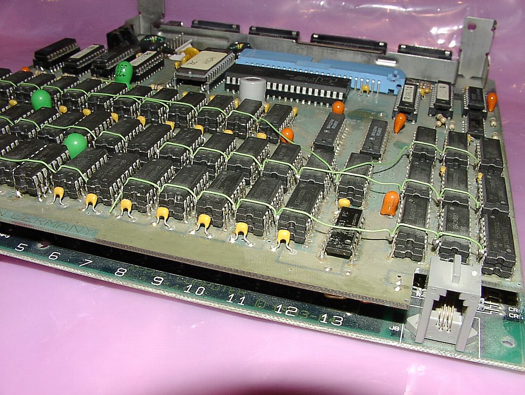
We were worried about the weak power supply and modified the DRAM refresh. The DRAMs onto the mainboard are also used for video. So this refresh rate could not be changed. But the refresh of the other three banks could be reduced to 1/9. My own Mac was a bit experimental and ran (out of spec) 1/11 without issues. The refresh cycles of the additional three banks were spread. Like that scheme:
cycle #0 bank 0 and bank 1
cycle #1 bank 0
cycle #2 bank 0 and bank 2
cycle #3 bank 0
cycle #4 bank 0
cycle #5 bank 0
cycle #6 bank 0 and bank 3
cycle #7 bank 0
cycle #8 bank 0
When testing the first board we were satisfied with the power consumption at all and looking at the peaks, and we were satisfied with the heat because the early Macs had no fan.
Re: OT: stacked (DIP) chips
Posted: Fri Jun 05, 2020 10:14 am
by BigEd
Ah thanks I see now. 112 total and I'd counted two drivers as rams.
Re: OT: stacked (DIP) chips
Posted: Mon Jun 08, 2020 6:04 pm
by Michael
Recently I hacked together a machined pin 6502 socket with integrated 0.8mm PCB and 64K RAM chip. The RAM gets all of its signals via direct connection to the 6502, except for the active lo chip enable which is connected to pin 35 on the socket (the 6502 "N/C" pin). The socket is intended to simplify breadboard wiring or PCB routing... Examples below;
Re: OT: stacked (DIP) chips
Posted: Mon Jun 08, 2020 6:12 pm
by Michael
Custom socket caveats are; (A) the 64K RAM chips I'm using are 5 volt only, and (B) pin 37 on the 6502 must be used for the system PHI2 clock.
Here's a couple more drawings;
Re: OT: stacked (DIP) chips
Posted: Sat Jun 20, 2020 2:03 pm
by argonn
Just a normal DIMM, 1GB DDR333 ECC REG
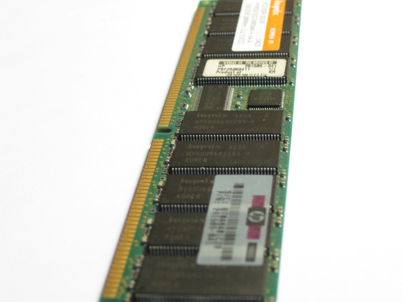
But wait!
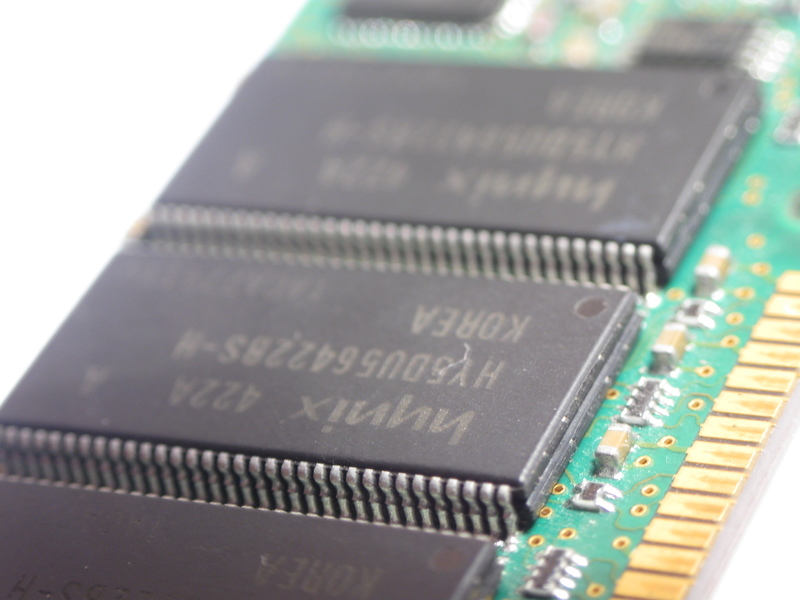
Probably designed to be mounted this way, all pins are connected between two chips, nothing is routed around. 36 memory chips, 40 chips total
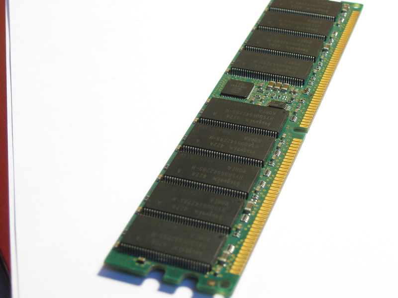
There were some 2GB DDR modules (also server ones) with additional PCB laminate layer so that some pins from the top layer were routed around. Things moved to BGA later, and started looking boring
Re: OT: stacked (DIP) chips
Posted: Sat Jun 20, 2020 2:56 pm
by Chromatix
I can only imagine there was an internal fuse to blow inside these chips to determine which select lines or addresses it would respond to.
Re: OT: stacked (DIP) chips
Posted: Sat Jun 20, 2020 3:10 pm
by BigEd
Could be that they had two bondouts, and two SKUs, and paired them up accordingly. (The unbonded pad would need an internal pullup or similar, but that's not much trouble.)
Re: OT: stacked (DIP) chips
Posted: Sat Jun 20, 2020 4:34 pm
by Dr Jefyll
Those are both plausible theories. But maybe the upper chips (and their plastic packages) have simply been spun 180 degrees, and the pinout is such that the spin results in no effective change for
most of the pins. But there's a Chip Select pin that ends up in parallel with a no-connect, and a no-connect that ends up in parallel with a Chip Select.
(Or perhaps an active-high CS that ends up in parallel with an active-low CS.)
Re: OT: stacked (DIP) chips
Posted: Sat Jun 20, 2020 4:50 pm
by BigEd
Ha ha - very inventive!
Re: OT: stacked (DIP) chips
Posted: Sat Jun 20, 2020 6:20 pm
by argonn
Those are both plausible theories. But maybe the upper chips (and their plastic packages) have simply been spun 180 degrees, and the pinout is such that the spin results in no effective change for
most of the pins. But there's a Chip Select pin that ends up in parallel with a no-connect, and a no-connect that ends up in parallel with a Chip Select.
(Or perhaps an active-high CS that ends up in parallel with an active-low CS.)
It looks that these are 256Mb 4b-wide chips (4 banks of 16Mbit x4 bits), so they probably routed data pins to some of NC pins of the other one, effectively getting 4 banks of 16Mbits x8 bits. Slightly less magical now.

Re: OT: stacked (DIP) chips
Posted: Sat Dec 19, 2020 11:48 pm
by plasmo
What would be awesome is if someone made a complete SBC (without the board) using nothing but stacked IC's.
And no micro-contollers or PLD's. :-)
I'm 2 years late responding to the challenge, beside I "cheated" by using a CPLD.
I was thinking about suspending a SBC by power, ground, and serial port wires and drives 3 circles of WS2812B RGB LEDs in the fashion of a clock. EPM7064S CPLD contains the serial boot ROM, serial port and glue logic; processor is Z80. The pin assignments of RAM and CPLD are flexible to simplify wiring. I need the processor to run at 22MHz which is multiple of 115200 and fast enough to bit bang the 1/3-2/3 pulse width modulation required by WS2812B. This mess actually works, but artistically it was a dud, so I never did build the clock. However, it was the inspiration for another SBC later, ZRC. I thought about this board again just this morning. With CPLD in 44-pin quad flat pack, the Z80 can fit over the CPLD and the RAM can fit under the board making a compact triple-stacked board. Hmmm...
The design and more pictures are documented here:
https://www.retrobrewcomputers.org/doku ... zorc:zorc0
Bill
Re: OT: stacked (DIP) chips
Posted: Sun Dec 20, 2020 10:08 am
by BigEd
Excellent construction!