Page 2 of 2
Re: 6502 SO-Pin / Chuck-Peddle-Special-Pin
Posted: Fri Jun 26, 2015 8:41 am
by Hobbit1972
The 74LS02 is a TTL part, a quite different process. Actually I'm not sure how good TTL is at pulling all the way up to the rail, but maybe it's fine.
Whoops - that points me to a little flaw in my breadboard design: no pull-ups, just TTL output of '02 into 6509... it seems to work... but maybe that's the reason for some quirks...
Re: 6502 SO-Pin / Chuck-Peddle-Special-Pin
Posted: Fri Jun 26, 2015 7:08 pm
by JimDrew
Interesting, I didn't think the 4040 was any different from the 8050/8250/1540/1541/1571/etc.
Re: 6502 SO-Pin / Chuck-Peddle-Special-Pin
Posted: Fri Jun 26, 2015 7:38 pm
by GARTHWILSON
Using RDY would be 2 clocks faster for it is already waiting inside the LDA. Using WAI would have to load LDA instruction, address byte (and possibly second address byte if I/O not in ZP).
That's an interesting idea. It would work if the input is transparent during the read, but the next thing to find out is whether the VIA will transfer
new data to the bus
during the read time, ie, data that wasn't there yet at the beginning of the read time.
Re: 6502 SO-Pin / Chuck-Peddle-Special-Pin
Posted: Sat Jun 27, 2015 1:31 am
by Dr Jefyll
the next thing to find out is whether the VIA will transfer new data to the bus during the read time, ie, data that wasn't there yet at the beginning of the read time.
Maybe I've misunderstood the context here, but I don't see how this is necessary. After every wait state (caused by RDY being low), another whole new bus cycle occurs (albeit to the same address). Seems to me the VIA should have no trouble delivering new data in the new bus cycle.
Re: 6502 SO-Pin / Chuck-Peddle-Special-Pin
Posted: Sat Jun 27, 2015 8:19 am
by BigEd
Hmm, are there reads of status registers which change the state, such that a repeated read isn't what you want?
I suspect the construction of the CS (or maybe the E input) to the VIA will determine whether it sees repeated reads or one looong read.
Re: 6502 SO-Pin / Chuck-Peddle-Special-Pin
Posted: Sat Jul 11, 2015 8:11 am
by Hobbit1972
Seems to me the VIA should have no trouble delivering new data in the new bus cycle.
I also would think so. VIA should sample data in phi1 and put the new data on the bus every phi2. But maybe somebody with a VIA could test it to be sure?
(If it would not work it should not be too difficult to find work around with RDY/CS logic.)
Hmm, are there reads of status registers which change the state, such that a repeated read isn't what you want?
That could be the case, of course - one has to keep that in mind.
On the other hand: in this design VIA's read or write handshake features probably are not too useful here, for it either triggers an IRQ or has to be polled by software - both completely unnecessary when waiting is already performed through RDY. Other accesses than to data Port A/PortB also is not used or necessary.
Re: 6502 SO-Pin / Chuck-Peddle-Special-Pin
Posted: Wed Aug 05, 2015 10:59 am
by i_r_on
You could use S.O. pin to do synchronous transfers. Trigger by hardware, use it in software type feature whereas RDY signal can only be used by hardware and you cant use it for synchronous transfers.
I guess the pin used initially for early testing & debugging of the design. And the least used flag is chosen as victim for this late addition to the design. (Just a guess)
Re: 6502 SO-Pin / Chuck-Peddle-Special-Pin
Posted: Tue Jul 15, 2025 3:16 pm
by wayfarer
could you use this as part of multiprocessing in bit slice form, ie:
6502 Lo has overflow, send Address or other Pin, to SO on 6502 Hi, and 6502 Hi can test this on certain operation chains.
Re: 6502 SO-Pin / Chuck-Peddle-Special-Pin
Posted: Sun Jul 27, 2025 5:32 pm
by fachat
All of the CBM disk drives used the SO pin, connected to the data separator. When a byte of data has been converted from flux to GCR, the SO pin goes low which sets bit 6 (V) of the flags. This has to be cleared in software (CLV) or you won't see the next one occur. This was used from the late 70's (PET drives) until the early 90's when CBM stopped producing the 1571.
I know this quite well, because it is what I am currently working on - a cycle exact CBM disk drive emulator using a PIC micro. I am emulating the 6502, two 6522's, 2K of RAM, and the data separator hardware with the proper crazy memory map that mirrors and has invalid (undecoded) addressing.
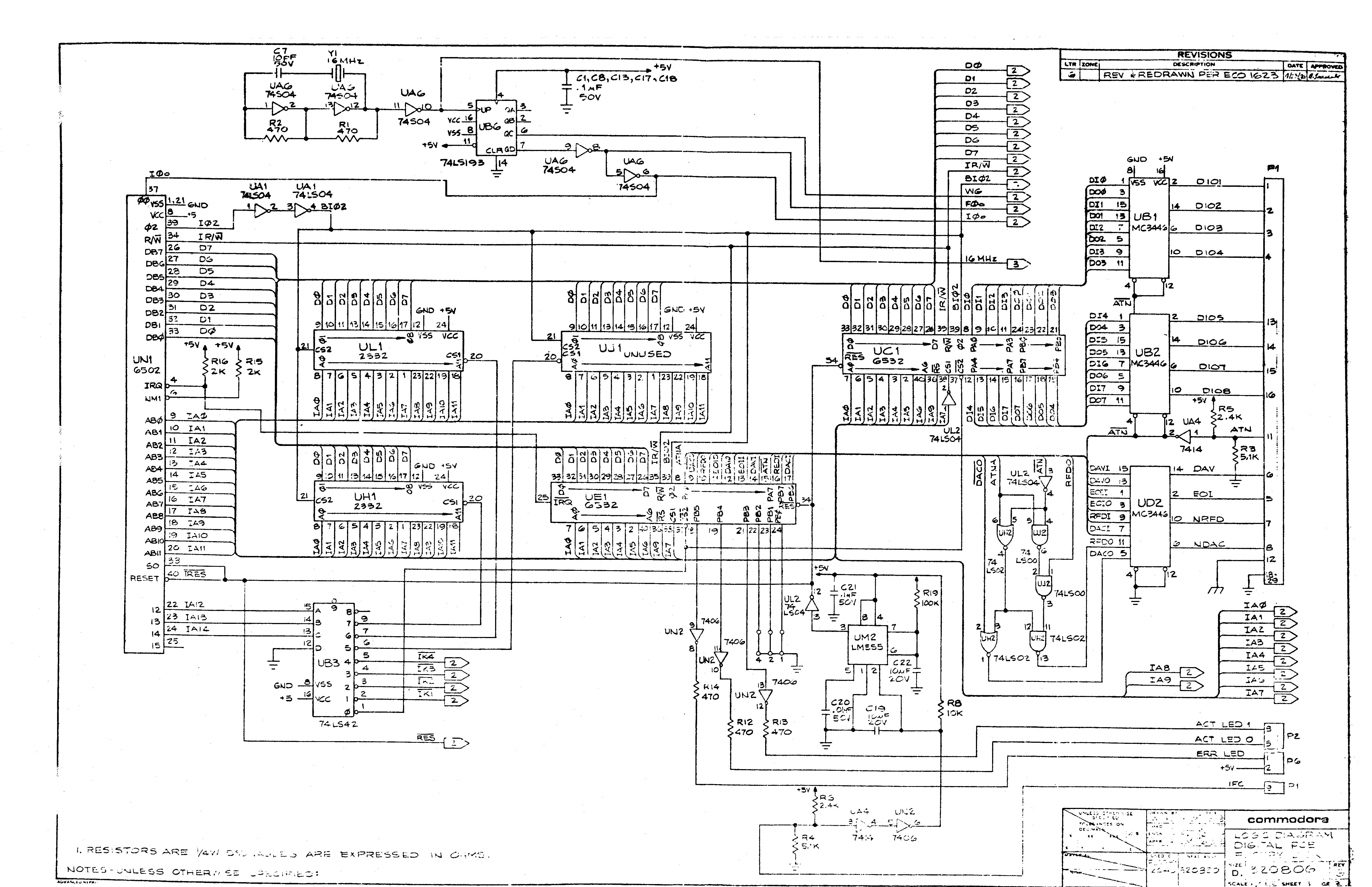
This is... interesting. Schematics for 4040 show that SO is pulled up, no connection to data seperator:
http://www.zimmers.net/anonftp/pub/cbm/ ... 0806-1.gif
and ROM code doesn't use SO therefore:
Code: Select all
 FDB1  24 4D     iFDB1      BIT VIA_IFR    ; get the bytes, store in (BUFPT),y, update checksum, jmp DEND
 FDB3  10 FC                BPL iFDB1
 FDB5  A5 41                LDA VIA_DIN
 FDB7  91 16                STA (BUFPT),Y
 FDB9  45 08                EOR WORK
 FDBB  85 08                STA WORK
 FDBD  C8                   INY
 FDBE  D0 F1                BNE iFDB1
"Byte ready" is tested via VIA. GCR decoding fully done in hardware. Checksum is generated within the loop.
Source:
http://www.6502.org/users/andre/petinde ... s1fdc.html
SO came into use in later series, 8250 for sure (didn't check with 8050 yet):
Code: Select all
FD9F          LFD9F:
FD9F 50 FE      BVC LFD9F
FDA1          LFDA1:
FDA1 B8         CLV
FDA2 A5 41      LDA io_diskdata_read_fdc
FDA4 91 17      STA (bufpnt_fdc),Y
FDA6 C8         INY
FDA7 D0 F6      BNE LFD9F
The guess would be that someone miscalculated the time available: 8250 has a higher data rate -- but still would leave plenty of time to do it the old way (no SO, test via VIA, checksum calculated later in a second loop), but the someone thought there would not be that plenty of time and tried to cut corners.
That's quite an interesting find! I didn't notice this before.
The 4040 (and 8x50) use a hardware GCR data encoder/decoder, reducing the data rate by 4/5. So there probably was enough time. The single CPU drives 2031/4031/1541/15x1 use software GCR en-/decoding, so the data rate was higher than the 4040. The 8x50 use a higher data rate in general even though still using the hardware GCR encoder. So they probably assumed that using SO was required to securely handle that increased data rate with the same 1MHz CPU clock.
André