Page 2 of 4
Re: Design of NEW 65Orgxx Devboard 'Backplane'
Posted: Tue Oct 16, 2012 4:19 pm
by BigDumbDinosaur
I just had the realization of using another one of ExpressPCB services to bring down the costs so that I may be able to purchase this board in a few days.
Using their Standard service, I can get 2 boards made for ~$100. The size limitation is gone also and the temptation was their to increase the number of PVB slots from 4 to 8, thereby maximizing pin usage from the control board connector. This increase in board size would be negligible in cost, however with the realization that in the past I have missed errors or have had other small oversights with all of my first attempts so far I will go ahead with the current design and hopefully put this order in 2 days. Definately, by next week though.
Yes, but the EPCB standard service product does not have silkscreen or solder mask. Are you okay with those features being omitted?
Re: Design of NEW 65Orgxx Devboard 'Backplane'
Posted: Tue Oct 16, 2012 4:44 pm
by ElEctric_EyE
Yes, but the EPCB standard service product does not have silkscreen or solder mask. Are you okay with those features being omitted?
Yes, which reminds me I have to do all my labelling on the top or bottom layers as the program does not take into account which service one uses, especially the use of silkscreen layer. Thanks BDD!
Re: Design of NEW 65Orgxx Devboard 'Backplane'
Posted: Wed Oct 17, 2012 3:24 pm
by ElEctric_EyE
Bit of a challenge to route the control signals from the 2 additional PVB's. It meant having to re-route the other 4 PVB signals, but it's done. The layout has been updated. Pin assignment tables will be updated before the end of today. Tomorrow I receive the new V1.0h PVB boards!
EDIT: Oh man, got them a day ahead of schedule, thanks ExpressPCB!
Re: Design of NEW 65Orgxx Devboard 'Backplane'
Posted: Wed Oct 17, 2012 4:41 pm
by BigDumbDinosaur
Tomorrow I receive the new V1.0h PVB boards!
EDIT: Oh man, got them a day ahead of schedule, thanks ExpressPCB!
Things must be slow at EPCB. 
Re: Design of NEW 65Orgxx Devboard 'Backplane'
Posted: Fri Oct 19, 2012 12:04 am
by ElEctric_EyE
Things must be slow at EPCB.
Yes, good for us, bad for them I guess.

. This is business though, better for them at least I order from them. They have an excellent service IMO.
Been thinking of the 'experimental CPU' that will be present on the controller board that will control the PVB's. Each PVB has a shared command bus 8 bits wide, has R/W and Phase 2 signals and will be WDC65C02/816 compatible, albeit at the 3.3V level.
At the low end one has 1 PVB, with no need of this Backplane board, with an 8-bit hardcore/softcore CPU, e.g. a WDC65C02 or WDC65C816 or 8051 or AVR or whatever one thinks is superior. I will personally be using possibly a modified 65Org16.b.
Re: Design of NEW 3.3V Devboard 'Backplane'
Posted: Tue Oct 23, 2012 12:30 pm
by ElEctric_EyE
This layout has finally solidified. I'll check it out for errors/changes again tomorrow and order 2 on thursday.
EDIT: One interesting idea I will be trying out once this mainboard is fully populated, is to make a special JTAG harness so ISE can see all IC's simultaneously, instead of having to plug and unplug the JTAG cable to each board in order to program them.
Re: Design of NEW 3.3V Devboard 'Backplane'
Posted: Thu Oct 25, 2012 1:20 pm
by ElEctric_EyE
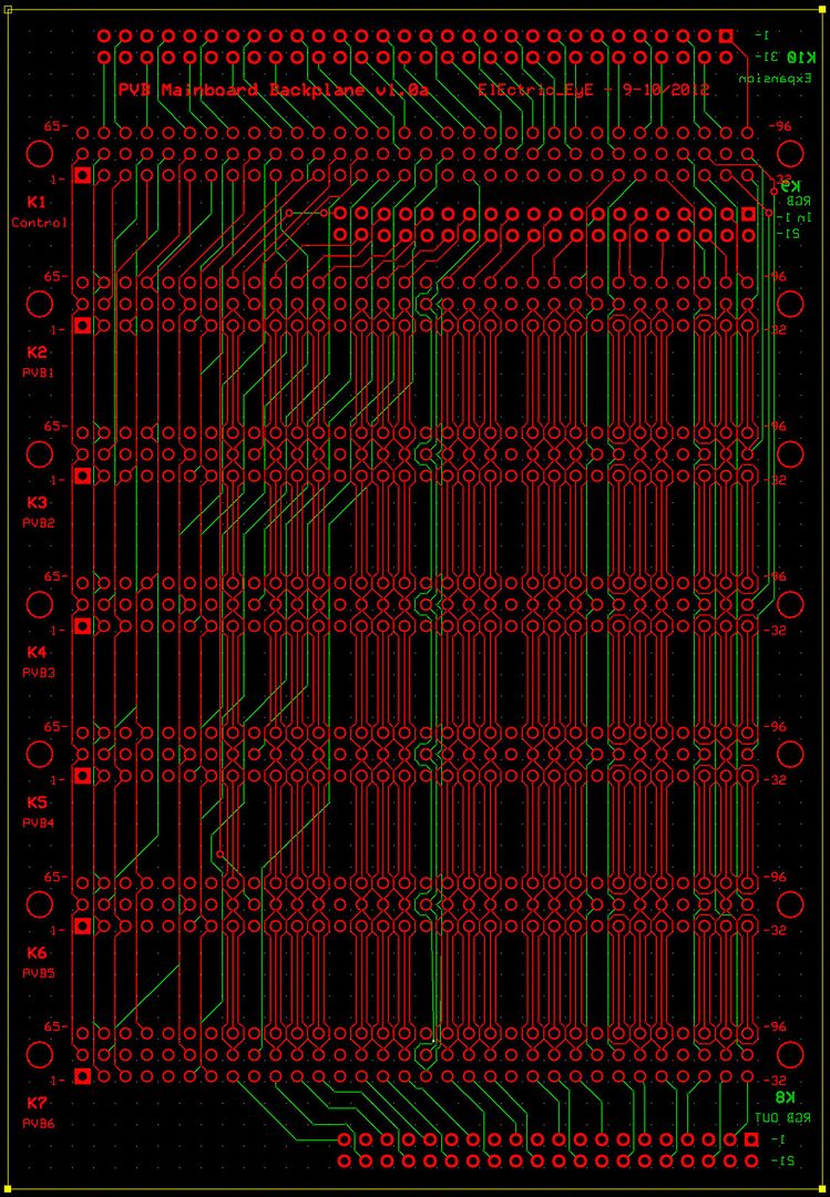
1 huge error I found was that I had the board selected as a 4 layer. So now there is no ground plane. Boards that will be connected to it will all be 4 layer though. Does anyone foresee a problem with this? Will it hurt signal integrity? The pic is updated at the head for what I am about to order.
Re: Design of NEW 3.3V Devboard 'Backplane'
Posted: Thu Oct 25, 2012 3:42 pm
by GARTHWILSON
1 huge error I found was that I had the board selected as a 4-layer. So now there is no ground plane. Boards that will be connected to it will all be 4-layer though. Does anyone foresee a problem with this? Will it hurt signal integrity? The pic is updated at the head for what I am about to order.
Am I looking at the wrong picture? I only see two layers in the one at the beginning (and the second row of each connector is mostly left unconnected). What are the rise times and expected frequencies? It seems to me that it would just be asking for trouble to omit the ground plane.
Re: Design of NEW 3.3V Devboard 'Backplane'
Posted: Thu Oct 25, 2012 3:49 pm
by ElEctric_EyE
Thanks for responding Garth, it's not that I'm omitting them. I had always planned on the 2 layer board after I decided not to route power through this backplane board. All the pins that are not connected will still be grounded by the 4-layer PVBs plugging into these receptacles. The price for a 4 layer board of this size would jump from $109 to ~$325 for 2! Can't afford that. Most frequencies around 100MHz. The one in the middle will be a main clock.
Re: Design of NEW 3.3V Devboard 'Backplane'
Posted: Thu Oct 25, 2012 4:25 pm
by GARTHWILSON
Then at least route ground traces to connect the ground pins from one connector to the next, between the signal traces. It looks like you have plenty of room to do it. Use vias if necessary. It doesn't do any good to have a gob of ground pins sprinkled around if they don't go through. The signals' return paths need to run really close to the signal traces, parallel to them.
Re: Design of NEW 3.3V Devboard 'Backplane'
Posted: Thu Oct 25, 2012 5:28 pm
by ElEctric_EyE
Ok, I follow you. I will do this for the high speed RGBin and RGBout and all clock signals. Thanks alot!
Re: Design of NEW 3.3V Devboard 'Backplane'
Posted: Fri Oct 26, 2012 12:21 am
by ElEctric_EyE
Garth, I've made some progress and I have another question if you would entertain it please: I think that the purpose of lining fast signals with grounds on either side, is to cancel out the EMI and other ill-effects. So would it be better, instead of using thin .006" traces, to go as thick as possible?
This is what I have so far. I have to figure out a few more things, but I'm thinking of doing away with the RGB I/O connectors.
Rambling here: For one, K9 the RGB-In connector is getting in the way of my primary clock signal from the K1 Control Board to the other PVBs on the bottom layer. RGB-in signals will ideally be coming from the controller board, from a video input module with 5-6-5 output into RGB-In. The RGB-Out at the bottom would be a different style connector, and would match pin spacing, in order to accomodate straight pass thru and signal protection for future HDMI output.
Re: Design of NEW 3.3V Devboard 'Backplane'
Posted: Fri Oct 26, 2012 1:20 am
by GARTHWILSON
Wide is good, but the first priority is just to get the return closeby. After that, the width and separation distance affect the transmission line's characteristic impedance, but at least the main problems with inductance and unwanted radiation and coupling are much improved. Again, it's not a matter of high-impedance electric-field capacitive coupling like we have more in audio, but of low-impedance circuits where magnetic fields are generated by current through a conductor. If the return path is right close to the signal path, the mutual inductance of the two will make equal and oposite currents flow in the two, cancelling out their effective inductance and their radiation. The balanced nature of it also reduces their susceptibility to unwanted interference. One of the effects of widening a trace is reducting the resistance that results from skin effect, but that's a pretty minor issue here. One of Dr. Howard Johnson's many articles on high-speed digital design deals with it.
Since your red (top) traces hide a lot of the green (bottom) ones, there's a lot we can't see, and seeing them would probably answer some things I find puzzling since I don't know all of what you're doing with it. Do take care of the green traces between PVB5 and PVB6 connectors however, near the middle, which have some pretty good design rule violations and unintended shorts to pads.
Re: Design of NEW 3.3V Devboard 'Backplane'
Posted: Fri Oct 26, 2012 2:01 am
by ElEctric_EyE
...Since your red (top) traces hide a lot of the green (bottom) ones, there's a lot we can't see, and seeing them would probably answer some things I find puzzling since I don't know all of what you're doing with it. Do take care of the green traces between PVB5 and PVB6 connectors however, near the middle, which have some pretty good design rule violations and unintended shorts to pads.
I can say what has happened naturally, is most of the slower signals were pushed to the bottom layer with considerable re-routing. All except for that 1 signal which is a 'potential' main clock. It is at the center of the board, and at the center of each connector on the bottom layer, the one that sticks out like a green thumb, with errors and shorts as you have noted. I had halted my progress and thought of getting rid of the RGB I/O connectors at this point because the RGB In connector is in the way of this primary signal... But thought I would post progress of my basic understanding of your hi-frequency signal protection.
Tomorrow, I'll focus on finishing the routing. Also, on filling in and widening the grounds around the hi speed signals. Thanks again for your continued input Garth!
Re: Design of NEW 3.3V Devboard 'Backplane'
Posted: Sun Oct 28, 2012 12:10 am
by ElEctric_EyE
I've updated the head post with a pic of what I have so far. The basic structure is still there, but alot of details have changed. I will work the errors out over the next few days. I post v1.0d at the head because I have a preliminary final design.
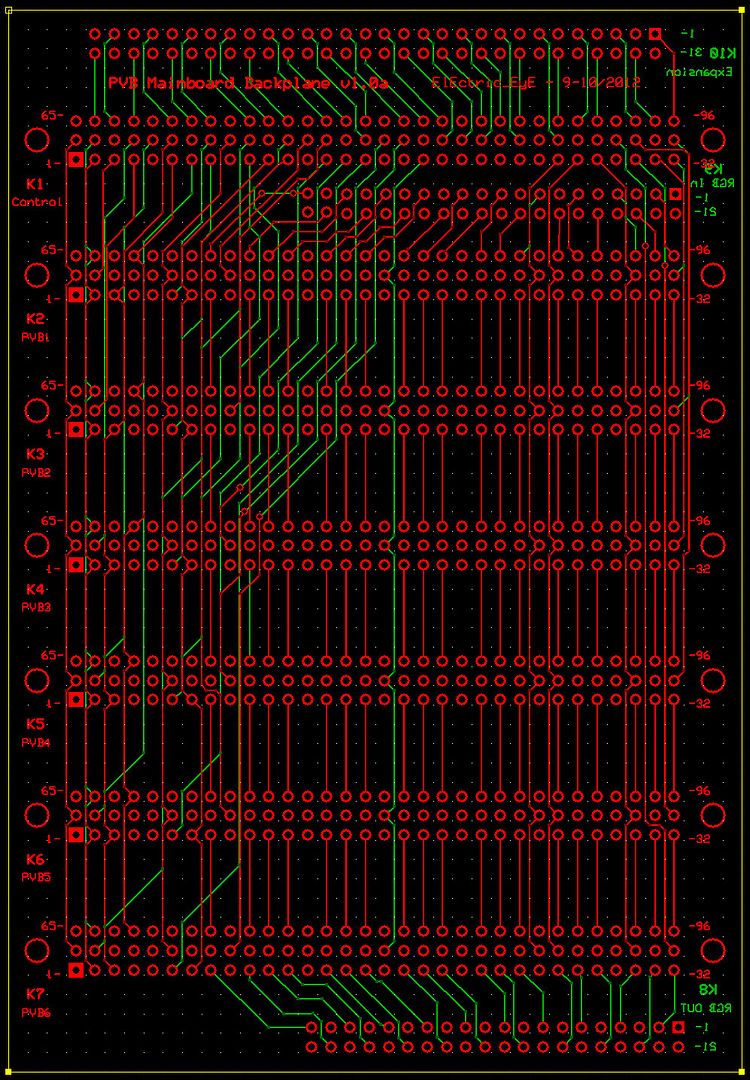
Here is v1.0c for comparison:
.