Page 2 of 15
Re: Breaking 6502 apart
Posted: Fri Jun 29, 2012 6:44 am
by org
That analog **** makes my research more complicated

Re: Breaking 6502 apart
Posted: Fri Jun 29, 2012 6:52 am
by BigEd
I think you can treat it all as digital, in the sense that a transistor is a switch. But it is bidirectional... And you can't divide up the circuit purely into neat logic gates. There are some interesting combinations.
By the way, the dynamic latches are the exact reason why a single stepping circuit must be careful about whether it stops with the clock high or low. One case will be fine, the other will have the leaking storage and will not be reliable.
Cheers
Ed
Re: Breaking 6502 apart
Posted: Fri Jun 29, 2012 6:56 am
by org
Thanks Ed, things become more clear to me.. )
50 kHz makes those 2 ms discharge rate )
At 500 kHz halfclock will last only 2us, its 1000 times shorter than discharge period )
So in order to recognize such capacitors I just need to pay attention on long polysilicon wires ?
Re: Breaking 6502 apart
Posted: Fri Jun 29, 2012 7:07 am
by org
Oh, I know.... When I see mosfets connected in parralel next time, I will add capacitor in schematics =)
Edit: like that :
Image no longer available: http://ogamespec.com/imgstore/whc4fed54d25dd47.jpg
Re: Breaking 6502 apart
Posted: Fri Jun 29, 2012 7:46 am
by BigEd
Well, you won't always have two transistors - in fact, usually you'll only have one. You'll see these nodes in the timing shift register in the first picture you posted - at top right there's a master-slave flip-flop made of two dynamic latches. More or less.
But you probably only want to annotate a capacitor when the latch is single and there's no recirculation.
Re: Breaking 6502 apart
Posted: Mon Jul 02, 2012 8:08 am
by org
Wrote small script which helps to understand which instructions are affected by decoder.
http://ogamespec.com/6502/decoder.htm
Type IR-line into input fiels and press "Decode". Script will highlight affected opcodes.
Example : XXX110X1
Re: Breaking 6502 apart
Posted: Mon Jul 02, 2012 8:30 am
by BigEd
Neat! It wasn't working for me at first, but I realised I was hitting 'Enter' rather than clicking on the button.
Re: Breaking 6502 apart
Posted: Mon Jul 02, 2012 7:23 pm
by org
Re: Breaking 6502 apart
Posted: Tue Jul 03, 2012 10:06 am
by org
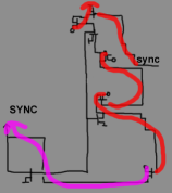
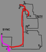
Todays speccy : SYNC
Color :
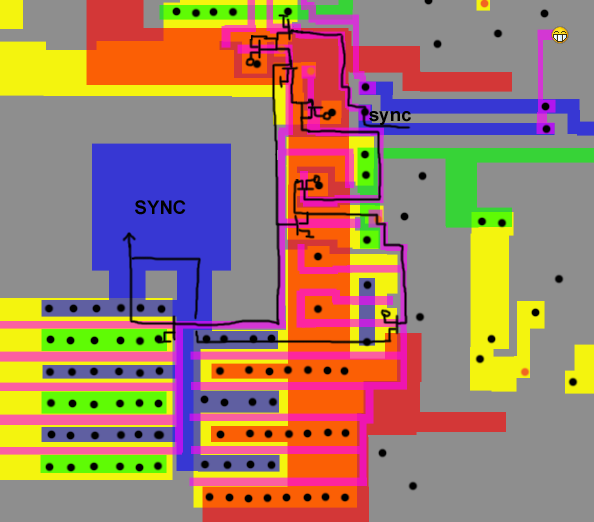
Transistor level :
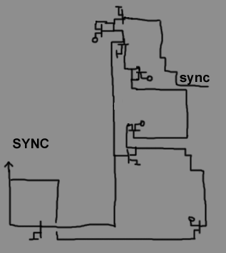
Logic:
SYNC = sync (driven by internal signal through amplifiers)
Re: Breaking 6502 apart
Posted: Tue Jul 03, 2012 2:18 pm
by org
Found error in data latch (missing vias).
Updated transistor level schematics :
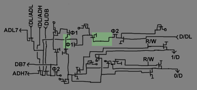
Re: Breaking 6502 apart
Posted: Tue Jul 03, 2012 5:42 pm
by org
I completed reversing of data bus logic

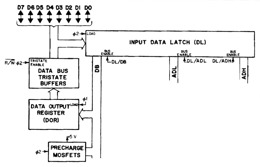
Code: Select all
PHI1:
if (DL_ADL) ADL = DL;
if (DL_ADH) ADH = DL;
if (DL_DB) DB = DL;
DOR = DB;

PHI2:
if (RW == 0) DATA = DOR;
DL = DATA;
ADL = ADH = DB = 0xFF;
Re: Breaking 6502 apart
Posted: Wed Jul 04, 2012 2:32 pm
by org
Started random logic
Simple explanation :

Re: Breaking 6502 apart
Posted: Thu Jul 05, 2012 8:43 pm
by org
Todays speccy : Registers X, Y, S
Color (bit 0):
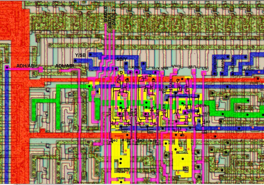
Transistor level:
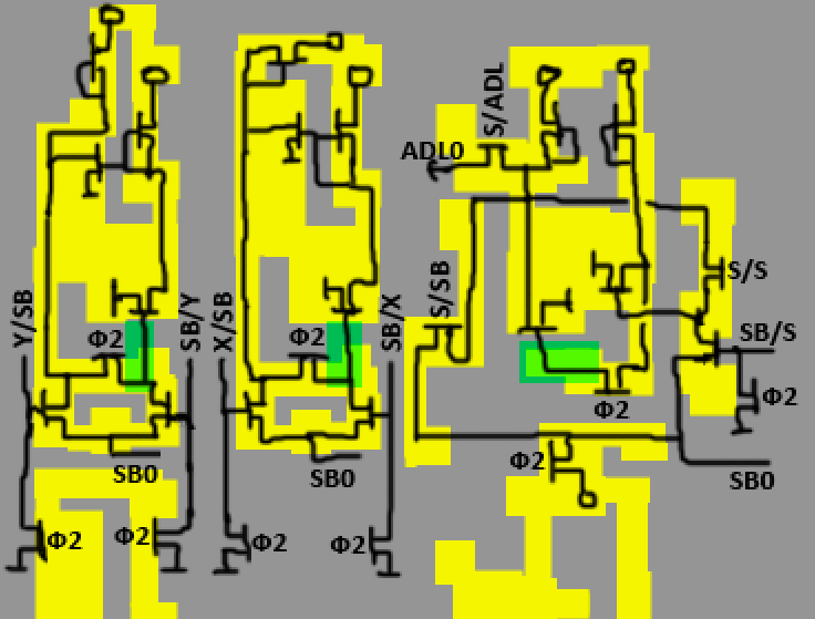
Logic:
Code: Select all
PHI1:
if ( Y/SB ) SB = Y;
if ( SB/Y ) Y = SB;
if ( X/SB ) SB = X;
if ( SB/X ) X = SB;
if ( S/ADL) ADL = S;
if ( S/SB ) SB = S;
if ( SB/S ) S = SB;
if ( S/S ) S = S;

PHI2:
SB = 0xFF;
Re: Breaking 6502 apart
Posted: Fri Jul 06, 2012 11:26 am
by org
Todays speccy : Predecode Register
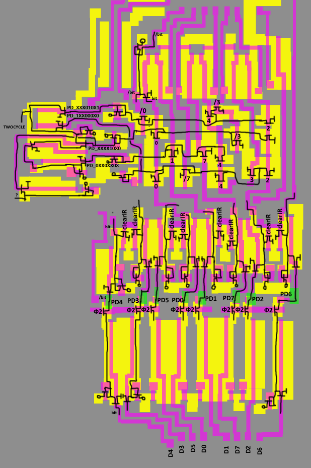
Re: Breaking 6502 apart
Posted: Fri Jul 06, 2012 11:56 am
by BigEd
Instantly recognisable! You notice how the first transistors from the databus are huge? I think that's to make the inverter's logic threshold a bit lower, which it needs to be because the databus is at TTL levels. Fortunately, it makes no difference to a logic sim. A big pulldown is a more eager one, so the output flips at a lower input voltage than it otherwise would.
You see the same thing in the next gate, after phi2, because the pass transistor transmits a degraded logic 1. The ClearIR inputs are normal sized by comparison. (As discussed previously, those PDn nodes are storage nodes.)
Cheers
Ed