Page 2 of 5
Posted: Thu Sep 16, 2010 9:49 pm
by BigEd
... interested in the 6800, because I'd like to see what similarities and differences exist ...
And the answer is...
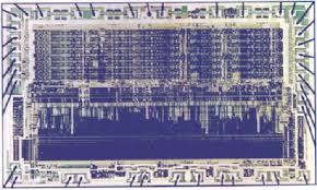
From
this patent: (US3987418A, now found
here)
 Viewed 4141 times")
- 6800 annotated chip floorplan
which compares to the 6502 (as seen at
visual6502):
 Viewed 1171 times")
- screenshot of visual6502 (early version)
...much less than I expected! I'm shocked!
Posted: Thu Sep 16, 2010 10:51 pm
by HiassofT
... interested in the 6800, because I'd like to see what similarities and differences exist ...
...much less than I expected! I'm shocked!
Hey, there's a very big difference! As we all can see from your pics, the 6800 was only black&white whereas the 6502 had plenty of colors :-)
gd&r, Hias
Posted: Fri Sep 17, 2010 2:08 am
by kc5tja
HAH, looks like Motorola was right after all. But, I'm still glad the 6502 won over the 6800.

Posted: Fri Sep 17, 2010 2:18 am
by ElEctric_EyE
What are the I5x pullouts from the die?
Posted: Fri Sep 17, 2010 5:37 am
by BigEd
What are the I5x pullouts from the die?
These are reference numbers (in the 150's) used in the text of the patent in the "Description of the invention" section.
I notice the patent text refers to many other patent applications submitted in the same timeframe, including on interrupts and on instruction look-ahead. One of the circuits I intend to investigate in the 6502 simulator is the lookahead - it looks like the databus is inspected and some pre-decode signals derived during the fetch cycle. If that's right, then it's stealing some nanoseconds from the external access time. It's possible this trick is inherited from the 6800.
I do have more named signals available than the released version of the simulator has - I imagine there'll be an update before long. I don't yet have the identities of the PLA outputs or the datapath control inputs, but I'll get them. We'll need a way to display or tabulate changes on all these signals too - presently I'm doing that by adhoc modifications to the javascript (pasted into the console at runtime)
Posted: Sat Sep 18, 2010 9:00 pm
by BigEd
Here's a curiousity -
this 65816 programming book has a die photo on the cover and it looks like a stretch-limo version of 6502. The datapath appears to be double length not double width:
- 65816 die photo from book cover
- 658162.jpg (12.83 KiB) Viewed 4403 times
Edit: replace lost imageshack-hosted image with attachment
Posted: Sat Sep 18, 2010 9:13 pm
by kc5tja
I think we pretty much knew that from its instruction timings.

update: smaller, faster, can load and run programs
Posted: Thu Oct 07, 2010 9:32 pm
by BigEd
The visual simulator just got faster and smaller (must be Moore's law)
There's also now a more low-level advanced interface, and by passing an appropriate URL you can load and run a short test program:
http://visual6502.org/JSSim/expert.html ... =60&r=0020
That particular program answers the riddle:
Q. When is the stack pointer not the stack pointer?
In this 'graphics=false' mode you can use the 'Show chip layout' button to explore the chip layout, where each conductor is coloured according to the logic level as the simulation progresses. '>' to zoom in, click and drag to pan.
Thanks to Greg, Barry and Brian for many of the new features.
Cheers
Ed
Edit: update link from pre-release to released area
Posted: Fri Oct 08, 2010 7:14 am
by RichTW
My first post here! Thanks a lot to the whole team for such an astounding piece of work; it's fascinating to see what's going on.
That's a curious thing that SP is trashed while executing a JSR (actually, I noticed this yesterday when I was playing about with 'expert mode', and thought it was some kind of bug in the frontend!). I wonder why it does that?
I have a question - what is the 'tcstate' column? First of all, I guessed it was the timer state (as sent to the PLA), but given that it barely changes (for example, during the JSR) and would be better represented as a series of bits, I guess not.
Posted: Fri Oct 08, 2010 10:02 am
by BigEd
Welcome!
Note that SP isn't trashed, it's borrowed for the LSB while the PC is written to the stack. During those writes, the value of SP must be decremented, so it spends a few cycles in the ALU - leaving the SP register free as a temporary!
The tcstate presentation is a bug, I'm afraid. It should show values like 011111, 101111 and so on, but I added the bits instead of concatenating them. There's a fix in the works!
(If you feel intrepid, you can find your browser's Javascript Console, get it to print out busToString, and adjust it to read
Code: Select all
function busToString(busname){
	// takes a signal name or prefix
	// returns an appropriate string representation
	if(busname=='cycle')
		return cycle>>1;
	if(busname=='pc')
		return busToHex('pch') + busToHex('pcl');
	if(busname=='p')
		return readPstring();
	if(busname=='tcstate')
		return ['clock1','clock2','t2','t3','t4','t5'].map(busToHex).join("");
	return busToHex(busname);
}
which is code you can
find on github
)
You should then see something like this tabulation:
Code: Select all
cycle  ab    db  rw  sync  pc    a   x   y   s   p         ir  tcstate  pd  adl  adh  sb  alu  alucin  alua  alub  alucout  aluvout  dasb
0      0000  a9  1   1     0000  aa  00  00  fd  nv-bdIZc  00  011111   ff  00   00   ff  00   0       ff    00    0        0        ff
0      0000  a9  1   1     0000  aa  00  00  fd  nv-bdIZc  00  011111   56  01   00   ff  ff   0       ff    00    0        0        ff
1      0001  00  1   0     0001  aa  00  00  fd  nv-bdIZc  a9  100111   56  01   00   ff  ff   0       ff    ff    0        0        ff
1      0001  00  1   0     0001  aa  00  00  fd  nv-bdIZc  a9  100111   ff  02   00   ff  fe   0       ff    ff    1        0        ff
2      0002  20  1   1     0002  00  00  00  fd  nv-bdIZc  a9  011111   ff  02   00   00  fe   0       00    00    1        0        00
2      0002  20  1   1     0002  00  00  00  fd  nv-bdIZc  a9  011111   df  03   00   00  00   0       00    00    0        0        00
3      0003  10  1   0     0003  00  00  00  fd  nv-bdIZc  20  110111   df  03   00   00  00   0       00    00    0        0        00
3      0003  10  1   0     0003  00  00  00  fd  nv-bdIZc  20  110111   ef  fd   01   ff  00   0       00    00    0        0        ff
4      01fd  00  1   0     0004  00  00  00  10  nv-bdIZc  20  111011   ef  fd   01   10  00   0       00    fd    0        0        10
4      01fd  00  1   0     0004  00  00  00  10  nv-bdIZc  20  111011   ff  fd   ff   ff  fd   0       00    fd    0        0        ff
5      01fd  00  0   0     0004  00  00  00  10  nv-bdIZc  20  111101   ff  fd   ff   ff  fd   0       ff    fd    0        0        ff
5      01fd  00  0   0     0004  00  00  00  10  nv-bdIZc  20  111101   ff  fc   ff   ff  fc   0       ff    fd    1        0        ff
6      01fc  00  0   0     0004  00  00  00  10  nv-bdIZc  20  111110   ff  fc   ff   ff  fc   0       ff    fc    1        0        ff
6      01fc  04  0   0     0004  00  00  00  10  nv-bdIZc  20  111110   fb  04   00   fb  fb   0       ff    fc    1        0        fb
7      0004  00  1   0     0004  00  00  00  10  nv-bdIZc  20  101111   fb  04   00   fb  fb   0       fb    00    1        0        fb
7      0004  00  1   0     0004  00  00  00  10  nv-bdIZc  20  101111   ff  10   ff   fb  fb   0       fb    00    0        0        fb
8      0010  e8  1   1     0010  00  00  00  fb  nv-bdIZc  20  011111   ff  10   00   fb  fb   0       00    00    0        0        fb
8      0010  e8  1   1     0010  00  00  00  fb  nv-bdIZc  20  011111   17  11   00   00  00   0       00    00    0        0        00
Cheers!
Ed
edit: SP is of course decremented, not incremented, for a push
Posted: Fri Oct 08, 2010 11:15 am
by RichTW
Note that SP isn't trashed, it's borrowed for the LSB while the PC is written to the stack. During those writes, the value of SP must be incremented, so it spends a few cycles in the ALU - leaving the SP register free as a temporary!
Ah, of course - that makes perfect sense! It's very cleverly and compactly designed.
The tcstate presentation is a bug, I'm afraid. It should show values like 011111, 101111 and so on, but I added the bits instead of concatenating them. There's a fix in the works!
That's great! I'll hang on for the next release
I'm intrigued by the tcstate - it doesn't seem to be quite as straightforward as it was originally made out to be.
Posted: Fri Oct 08, 2010 11:22 am
by BigEd
The tcstate presentation is a bug, I'm afraid. It should show values like 011111, 101111 and so on, but I added the bits instead of concatenating them. There's a fix in the works!
That's great! I'll hang on for the next release :) I'm intrigued by the tcstate - it doesn't seem to be quite as straightforward as it was originally made out to be.
Indeed, it's an interesting area. The Rockwell docs describe a simple counter, but this MOS chip certainly doesn't have that - and I think this might be universal at least up to 65CE02. What we really have is a bitvector, which drives some of the wordlines of the PLA. The last 4 of these do seem to be a shift register, but the first two are more free than that. That's why I wanted to present the set as a bitvector.
Note also that in the Sync cycle, the IR still holds the previous instruction and the machine is still acting on that. It's a simplification (at best) to think of this as T0 of the instruction being fetched. From the point of view of the programmer's model it's good enough, but if you insist on thinking that way down at the microarchitectural level, you might conclude that the 6502 can't be built!
Cheers
Ed
Edit: spello
Posted: Mon Oct 18, 2010 1:50 pm
by ElEctric_EyE
Big Ed, does the visual6502 team plan to release any of the netlists of the devices being preserved?
Posted: Mon Oct 18, 2010 2:11 pm
by BigEd
yes, at least in the sense that the netlists already get downloaded and used by your browser when you visit the site!
Now, what you actually download are javascript files, with some comments, which between them tell you which transistors are connected to which nets, and gives you some names for some of those nets - including the pads of course.
What you don't get is a netlist in a recognisable form, like SPICE or Verilog. Also, you're getting transistors, not logic gates. Some of the transistors form easily recognisable logic gates, but some don't, because there are some non-obvious but efficient ways of building shared busses and latch structures.
If there were a good standard format for transistor level netlists someone could probably rustle up a conversion fairly easily. Irsim seems like the right sort of (free) simulator, but I don't know anything about the netlist formats it supports.
What did you have in mind? (Those transistor-level tricks make it tricky to see how to port to an FPGA.)
Posted: Mon Oct 18, 2010 3:08 pm
by ElEctric_EyE
Yes, I was thinking of implementing the netlist file as a symbol representing the IC. Heh, I knew the idea sounded to easy to work.
-EyE