Page 10 of 17
Posted: Tue Aug 09, 2011 1:12 pm
by ElEctric_EyE
Arrgh! I laid out the wrong style package for the memory. Spacing on the board is .025", but the package is .03149" (.8mm) pin spacing. Major bummers, I was hoping to do some experimentation with SDRAM. Not only can't I do this, sizing up this much larger IC, but for the next version if it were to remain onboard I would have to lose the serial EEPROM, or maybe if I can fit it on the other side. I will have to see later. Hopefully the rest will work...
This morning I finished up all the other IC's with my butane micro-tip iron. Gotta finish up the headers, connectors, then start in on the 0605 stuff! Maybe can power up and test JTAG tomorrow...
New SMD soldering station won't be in till thur. Will comment on it soon...
EDIT: fixed correct pin spacing
Re: Fine Pitch Slobbering
Posted: Tue Aug 09, 2011 3:55 pm
by BigDumbDinosaur
...I fooled around with using my small heat gun (has a vacuum cleaner style nozzle) to reflow a SOJ32 part...
So was this a new board you soldered the part to? and you didn't have to add any solder?
Correct. All I did was flux the pads and pins. There was enough reflow on the PCB to make a good joint.
I've used the .015" solder because it was so thin, not because it was silver bearing solder, and I could get such a small amount on the solder tip. It transferred solder to about 10 pins before I had to use more.
Oh. I thought you were soldering through-hole parts with this stuff.
Posted: Tue Aug 09, 2011 8:54 pm
by ElEctric_EyE
I was impatient today and decided to try to assemble the whole thing in one shot. During my trials and errors I decided to lose the butane micro-tipped soldering iron. It just didn't get hot enough. I actually used my big fat soldering iron on the 0605 parts. Just had to hold down the cap's and one small application of high heat and a puff of smoke with hardly any .015" solder, bam a nice clean connection. This was after initially soldering 4 caps using the smaller soldering iron and after I almost punched a hole in the wall.
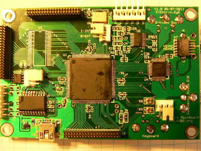
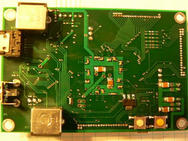
Anyway, I measured 17ohm resistance between 3.3V and GND and .4 ohms between 1.2V and GND. So there is a big time short after soldering. On the other 2 bare boards there was infinite resistance. So I screwed up "slobbering"somewhere. In retrospect, I should have take resistance readings after soldering each part... Not only that, I noticed resistors for the PS2 keyboard and the S-Video connector are underneath the connector. They need to be on the top side. So all these factors in combination with the fact that I can't even fit the SDRAM on this board forces me back to the drawing board for version 1.1. Sorry for the letdown folks
But I will take a pic of both sides just for the hell of it.
Posted: Tue Aug 09, 2011 9:25 pm
by BigEd
Pity about the SDRAM thing - can you shake out any more bugs, now that you have the boards in your hands? Is it still worth populating one of them with most of the other parts or are you heading straight for a 1.1 revision?
Cheers
Ed
Posted: Tue Aug 09, 2011 10:27 pm
by ElEctric_EyE
Hi Ed,
I plan on deconstructing this board 1 part at a time until I find out where the 1 hard short (.4ohm) and a semi? short (17ohms) are. In the pic's the 1.2V reg has been removed already. It was getting hot and the Spartan 6 was getting warm after about 20 sec's. These 2 IC's unfortunately have been sacrificed. But if I can learn what not to do, then it's a worthwhile experience. All I plan on salvaging are the connectors from this thing...
This is a totally new beast to me as far as prototyping. I used to prefer wirewrapping, but the cost of SMD adapters equal if not surpass the cost of manufacturing 3 boards. Bear with me. Anyway here are the pics as promised, before further deconstruction...
Top:
Bottom:
Posted: Tue Aug 09, 2011 10:47 pm
by ElEctric_EyE
BigEd wrote:
Pity about the SDRAM thing - can you shake out any more bugs, now that you have the boards in your hands? Is it still worth populating one of them with most of the other parts or are you heading straight for a 1.1 revision?
Cheers
Ed
I would have liked to solidfy the JTAG jumpers. I may still have a chance... Today's IC's are very forgiving. Although the Spartan 6 was getting warm, it wasn't dissipating heat like the 1.2Vreg, , and I only had GND & 3.3 voltage applied for a very limited time...
1 question? If one of these SMD caps did blow out, could it become a conductor? I could have sworn I heard a small pop as soon as I initially plugged in 3.3V, but it was very faint so I'm not sure...
Posted: Wed Aug 10, 2011 10:21 am
by ElEctric_EyE
I'm starting to think maybe it's the extreme liberal way I applied the solder flux to the board with a cotton swab to help keep the caps in places. I did clean up the flux around the parts using acetone, but I can't get underneath.
I think next attempt I put the flux in a needle (wife used to take shots, I have one or 2 around) maybe very briefly heat up the metal needle tip and put the smallest drop on each pad, then place the part.
Another concern is maybe the first 4 caps on the topside got damaged from too much heat, I was really struggling with getting a routine down. That is, incidentally, the 1.2V bypass caps which I intend to remove first.
Heh, I am up very early this morning thinking out loud about this dilemma. Can't turn on the lights yet, family still asleep.
Also, I did notice the the .1uF caps had a place to solder on the sides of the package creating a possible short, so I removed all those caps and am using the .01uF.
Posted: Wed Aug 10, 2011 5:11 pm
by Arlet
For new boards, I usually work in stages. First try to get power supplies working, oscillators, and then add main ICs one at a time. Every time I add something, I test and measure to see if it works.
It takes a bit more time that way, but if a short develops in a supply net, you have a good idea where to look.
Posted: Wed Aug 10, 2011 6:27 pm
by ElEctric_EyE
Yeah, I rushed it and paid a price. I blew out the Spartan 6.
Focusing on the 1.2V .4ohm short to ground, I removed all the VCCINT bypass caps. That 1.2V supply only goes to 5 pins on the entire board. Still, removing these caps did not remove the short. After surgically removing all of the VCCINT pins from the Spartan 6, the short to GND disappeared, proving I let the smoke out of the Spartan 6. Poor thing...
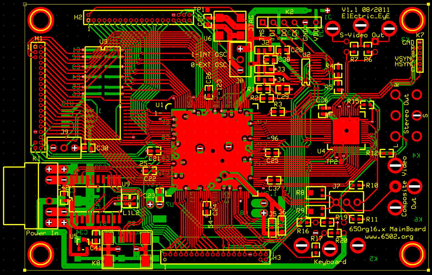
I'm now busy with V1.1 of a new PCB. It will have a correct template for the SDRAM and just a few other placement corrections. Turnaround will be much quicker than V1.0.
I also will have the correct tools and will take it slower this time and measure resistance on each of the power lines with respect to GND and with respect to each other, after soldering each and every part!
Posted: Thu Aug 11, 2011 2:58 am
by BigDumbDinosaur
I'm starting to think maybe it's the extreme liberal way I applied the solder flux to the board with a cotton swab to help keep the caps in places. I did clean up the flux around the parts using acetone, but I can't get underneath.
You shouldn't use acetone to clean up. Aside from the fact that acetone is extremely flammable and can cause a flash fire, it will damage the solder mask and possible delaminate the board layers. Isopropol alcohol, sold as denatured alcohol solvent in hardware stores and paint shops, is the preferred solvent for cleanup.
Do be a bit sparing with the flux. Try to confine it to the pads to avoid making it easy for a bridge to form during soldering.
Re: Fine Pitch Slobbering
Posted: Fri Aug 12, 2011 7:00 pm
by ElEctric_EyE
BigDumbDinosaur wrote:
ElEctric_EyE wrote:
BigDumbDinosaur wrote:
...I fooled around with using my small heat gun (has a vacuum cleaner style nozzle) to reflow a SOJ32 part...
So was this a new board you soldered the part to? and you didn't have to add any solder?
Correct. All I did was flux the pads and pins. There was enough reflow on the PCB to make a good joint.
Now I am curious what temp you had the hot air up to? and for how long before you saw the solder flow?
I got my SMD resoldering station last night and can give this technique a try.
Re: Fine Pitch Slobbering
Posted: Sat Aug 13, 2011 5:04 pm
by BigDumbDinosaur
...I fooled around with using my small heat gun (has a vacuum cleaner style nozzle) to reflow a SOJ32 part...
So was this a new board you soldered the part to? and you didn't have to add any solder?
Correct. All I did was flux the pads and pins. There was enough reflow on the PCB to make a good joint.
Now I am curious what temp you had the hot air up to? and for how long before you saw the solder flow?
I got my SMD resoldering station last night and can give this technique a try.
I have no idea what the temperature is. I just let 'er rip until the solder flowed, at which time I shut off the gun and let the parts cool. Yes, more than crude, but no loss to me if the SRAM was damaged. I'll know as soon as I populate the board and hook it up.
Posted: Sat Aug 13, 2011 11:56 pm
by ElEctric_EyE
I decided against the hot air at this point, even though I can control the temp. I still prefer the application of solder, even though it be the slightest amount, especially for higher amp ICs...
Ah how sweet it is! With the right tools, the job is so much easier! I have the soldering station I previously mentioned. Also a medical type needle dispensing the smallest amount of flux with the sharp tip cut off for a nice clean application.. So to get this crazy train back on track:
I desoldered the 2.5V reg from the faulty board (what a breeze!) and soldered it and a new 1.2V reg to the 2nd of 3 V1.0 boards I have left.
I was measuring a 13ohm load on the 2.5V vs. the .4ohm on the 1.2V reg, so the 2.5V reg is probably still good. More are on order, but it's the only one I have right now...
I aim to solidify a JTAG schematic for V1.1, so I can eliminate alot of wasted space due to all the jumpers. This may require some experimentation, but hopefully not too much. I've read the Xilinx forums... and my first test, hopefully successful, only involves 2 resistors.
Posted: Tue Aug 16, 2011 3:19 pm
by ElEctric_EyE
Done resizing and rerouting the correct SDRAM package for
V1.1 board layout, and a few placement corrections of quite a few things...
The SDRAM data lines flow much better than V1.0.
Also, I was able to keep the serial flash. Should be enough storage for 512K+x16bits.
I will need to update Header info and the schematics.
Now on to more soldering and testing so I can solidify V1.1...
Board Density
Posted: Tue Aug 16, 2011 4:59 pm
by BigDumbDinosaur
Done resizing and rerouting the correct SDRAM package for
V1.1 board layout, and a few placement corrections of quite a few things...
What size traces are you using? It appears you could go down on the size of a lot of them and reduce stray capacitance in many areas. Since this appears to be an EPCB 4-layer design, you can go as small as 0.006 inches on signal traces and as small as 0.026 inch with the via. It's been my experience that the smaller traces make it easier to increase trace separation in dense areas, which will help keep a lid on crosstalk between adjacent circuits.
Also, if it were me, I'd dispense with the filled planes. The internal power and ground layers act as a giant bypass capacitor, so interlayer crosstalk will be negligible and the filled planes won't be doing anything useful for you. What they may do is add to the stray capacitance and possibly mess up a signal whose trace has to pass through the plane.
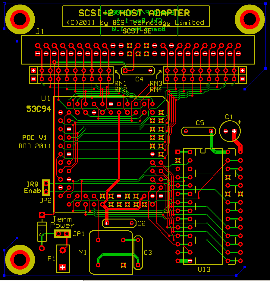
Here's what I did for the
SCSI host adapter daughterboard for my POC unit. With the exception of the traces going to the SCSI bus receptacle (top of layout) and a few others, all traces are 0.006 inch and via are 0.026 inch. This 4-layer board measures 3-1/8 inches wide by 3-1/4 inches high before routing to the final shape. The SCSI ASIC is a PLCC84 package.