Page 9 of 15
Re: Breaking 6502 apart
Posted: Thu Nov 15, 2012 1:34 pm
by org
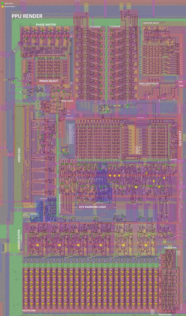
I already simulated some parts of random logic, but attracted by NES PPU

Technically I understand whole random logic, just need to simulate it carefully step by step.
The reason I turned my attention to the PPU : I want to see some visuals

Because you can effectively ignore most of custom NES CPU hardware and get some picture just from 6502+PPU bundle.
Here is my new circuit drawing style (transistors over dim background + highlighted regions), to demonstrate complexity of reverse engineering circuits I do

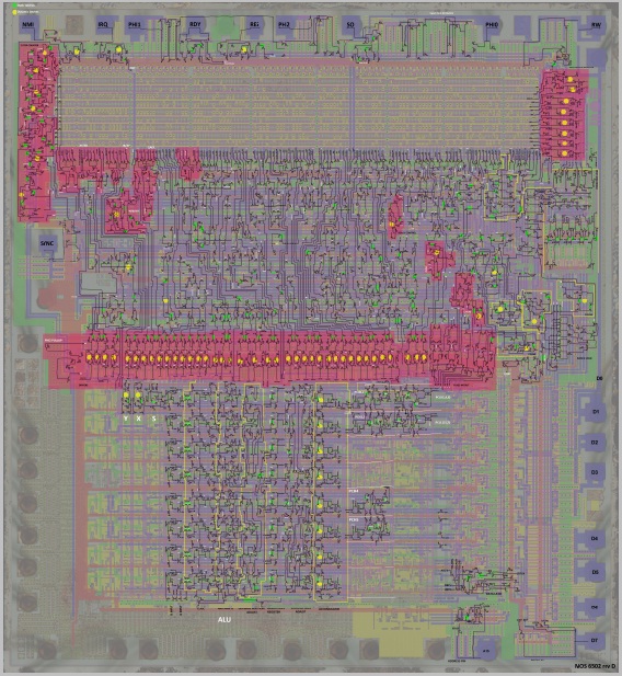
I gonna restitch 6502 circuit by the same way.
Re: Breaking 6502 apart
Posted: Thu Nov 15, 2012 4:40 pm
by Zetmor
Wow, that's a huge job you made org.
I really need to learn to "read" those schematics so that I can (someday) simulate those NES chips.
(would do it at logic level, with basic gates like OR/AND/NOR/NAND/NOT ...)
Re: Breaking 6502 apart
Posted: Sun Nov 18, 2012 10:14 pm
by org
You still need to use transistors as transfer gates ("enablers/disablers" transistors) and for static latches, when MOSFET gate is in floating state, keeping its charge and locked by transfer gate. So you cant do it by basic gates only.
Re: Breaking 6502 apart
Posted: Wed Nov 21, 2012 2:46 pm
by org
Ignore my previos post, its possible
Static latches are actually D-triggers, but transfer gates are just tri-states:
http://en.wikipedia.org/wiki/Tri-state_logic
So, I'm gonna rearrange my transistor circuits into logic schematics

Restitch in progress :
I decided to complete following parts:
- redraw PLA as NOR gates
- add missing address/data latch registers and pads (they are just regular and same as A0/D0, so do copy paste)
- add missing X/Y/S and PCH/PCL register bits
- add missing predecode logic lines ) (the are also same as PD0, I was lazy to draw it before)
After working on NES chips I have a fresh view on 6502 (especially on logic representation of transistor arrangements)
Re: Breaking 6502 apart
Posted: Wed Nov 21, 2012 10:12 pm
by org
I'm again with you
(clickable)
By removing interconnection wires I improved circuit readbility A LOT
Also I found and marked many interesting regions
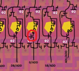
Green-square latches are D-triggers, while yellow hexagons are RS-triggers. Random logic output has many of them, as well as flags, intruction register and cycle counter.
Re: Breaking 6502 apart
Posted: Wed Nov 21, 2012 10:25 pm
by BigEd
> Green-square latches are D-triggers, while yellow hexagons are RS-triggers
That's visually very helpful!
A note on terminology: I'd say D-type [transparent] latch and RS-flop (or RS-flip-flop) - but I think often in the 6502 we see a master-slave flop rather than an RS. Having said that, I may be using the wrong terms, and other variations may exist!
Cheers
Ed
Re: Breaking 6502 apart
Posted: Wed Nov 21, 2012 10:41 pm
by org
That doesnt matter, since I understand it in different way )
Green one latches are SRAM-type memory (floating gate keep its charge) and yellow flip-flops are DRAM-type cells
Re: Breaking 6502 apart
Posted: Wed Nov 21, 2012 10:46 pm
by BigEd
Is that the other way around? A DRAM cell is a single transistor, which is your green one (a D-type latch) whereas an SRAM has two re-inforcing inverters (usually) which is quite like the yellow one, except I think the yellow ones are clocked - certainly some of them are. In fact, you'll see a difference between the cells of the stack pointer S and the cells of the X and Y registers.
Cheers
Ed
Re: Breaking 6502 apart
Posted: Wed Nov 21, 2012 11:41 pm
by org
Yeah, thats otherwise )
Re: Breaking 6502 apart
Posted: Fri Nov 23, 2012 10:56 am
by org
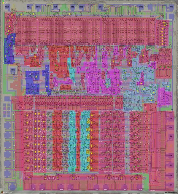
Todays speccy: random logic propagation map.
It helps me to construct propagation priority table, to simulate different parts of random logic in correct order.
Re: Breaking 6502 apart
Posted: Fri Nov 23, 2012 12:54 pm
by BigEd
Very nice - and the first time I've seen anything like this!
Does this mean you will also be able to tell us which paths are the longest? That would be after you've sorted out the program counter, I suppose.
(The longest in terms of gate count is not necessarily the slowest, of course.)
Cheers
Ed
Re: Breaking 6502 apart
Posted: Fri Nov 23, 2012 3:09 pm
by org
If you look down to "driver" outputs, you may notice, that output lines are buffered by PHI2.
So, during PHI2 they are loaded by new values, and during PHI1 they are simultaneously outputs.
Also, most of flip-flops has PHI2 cutoff at the output, so those lines are effectively disabled.
But some lines has except (example is S/ADL), which has valid output during both PHI-stages.
I think, you can assume, that all lines are fired simultaneously and those weird undocumented opcode behavior depends on bus conflict issues.
Re: Breaking 6502 apart
Posted: Mon Nov 26, 2012 10:35 am
by org
6502 simulation already done.
I have implemented almost all random logic in form of C code.
Please again ignore my previous post
, because I was wrong - random logic outputs are NOT using RS-like latches (I thought it was depletion-mode transistor but it was simply pullup ).
As you already noticed, other RS-like formations (flags) are not really "flip/flops". They are just some transient circuits, which are "loaded" during PHI2 and "read-back" during PHI1. Such pass-through gates are need to eliminate unwanted read-back conflicts during "load".
Also I (possibly) found a glitch in program counter swapping (well, not actually glitch
just some specific 6502 inner working). The reason is program counter put its value on ABH/ABL and loaded back in inverted form back again, to compensate swap, which occure every half-clock.
After I complete random logic, I show you opcode lifetime sequence (which "commands" random logic dispatch to bottom part per cycle).
Reset sequence is simply sort of BRK (its already known though), since instruction register is 0x00 after reset.
I found, that stack register keep its value in inverted form, so its value after power-up is NOT(0x00) = 0xFF (extended to 0x01FF). When stack register value is loaded from the bus (and written back), it get pre-inverted.
Re: Breaking 6502 apart
Posted: Wed Nov 28, 2012 6:45 am
by enso
This is really excellent.
Re: Breaking 6502 apart
Posted: Fri Nov 30, 2012 5:48 pm
by Zetmor
Yep, wonderfull!
I really need to take the time to do my logic sim (realtime on CUDA), and try to simulate that one!

