6502.org Forum  Projects  Code  Documents  Tools  Forum
It is currently Mon Jul 01, 2024 2:06 am

All times are UTC


Post new topic Reply to topic  [ 224 posts ]  Go to page Previous  1 ... 5, 6, 7, 8, 9, 10, 11 ... 15  Next
Author Message
 Post subject:
PostPosted: Wed Mar 02, 2011 12:57 pm 
Offline

Joined: Mon Mar 02, 2009 7:27 pm
Posts: 3258
Location: NC, USA
I don't know why I kept thinking 45MHz as the default frequency of the DS1085-5. It's 48.58MHz. So rewriting the constraint below (after some other fiddling) worked @ 24MHz! I always seem to have the greatest success in the mornings.:D. Now if I can get the display to run @48MHz, I will be very happy indeed.

Code:
NET "O2" TNM_NET = O2;
TIMESPEC TS_O2 = PERIOD "O2" 20.5 ns HIGH 50% INPUT_JITTER 100 ps;
NET "O2Out" OFFSET = OUT 5.5 ns AFTER "O2" RISING;


---------------------------------------------------------------------------------------------------------------------------------------------------------------------------------------------------------------------------------------------------------------------------
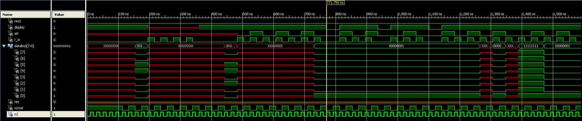
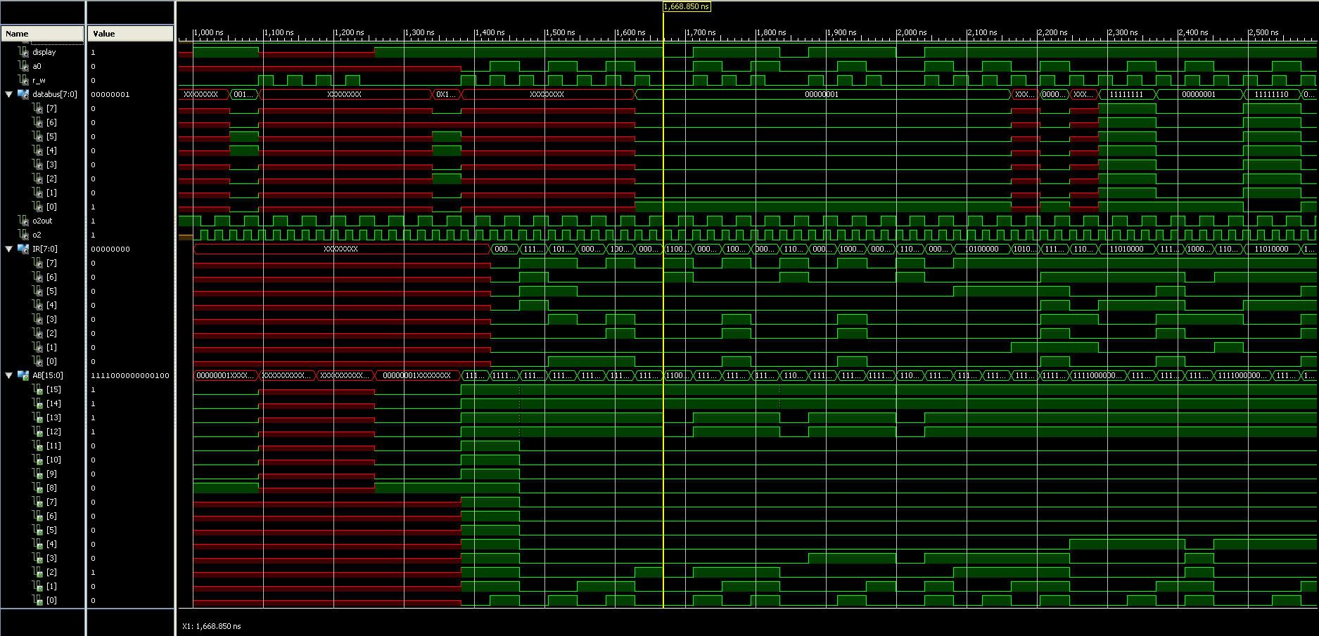
I was abit premature in my declaration of success 7 hrs ago. I later realized I had a timing constraint error because my 5.5ns "estimated" delay is shorter than the internal delay (as spec'd by ISE), from O2 to pad, of 11.7ns. Although the circuit still worked the best I had so far, it was locking up after some time (<1min)...
After looking over some of my old schematics from the PWA project, I decided to qualify WE from Arlet's 6502 core with O2/2. In addition, instead of an arbitrary 5.5ns, I calculated the actual time I needed to put O2Out in sync with O2, although the display likes an inverted version of O2.
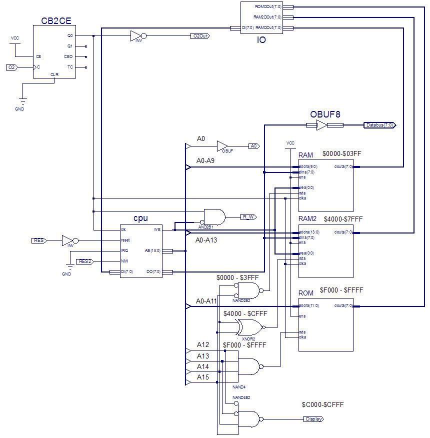
The 6502SoC has been running now for over an hour with no problems @24MHz using this constraint with the schematic below:
Code:
NET "O2" TNM_NET = O2;
TIMESPEC TS_O2 = PERIOD "O2" 20.5 ns HIGH 50% INPUT_JITTER 100 ps;
NET "O2Out" OFFSET = OUT 19.0 ns AFTER "O2" RISING;
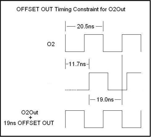

As I am not a timing diag kind of person, I realized in the middle of posting this, that the diagram below is incorrect. The 2 waveforms below O2 are divided by 2 in the schematic. As usual with me, I happen across my successes sometimes by accident. This "accident" will give me insight to pushing for 48MHz, because for sh*ts and giggles I just now tried to run the 6502SoC @48MHz, and it cleared the display. Although repeatability was not there yet, it did more now than previous attempts @48MHz... I'm zeroing in!
Image
Updated schematic:
Image
Note(s) to self: After reading this post on my 2nd favorite forum, Xilinx forums, Austin Lesea (their principle engineer) comments on jitter value ranges. "...100ps for synchronous design with single clock...", and "...1000ps for... poor bypassing...".
A video about switch debouncing an FPGA.
A video about someone with similar ideas to mine using an XC3S400, T65 core, PS/2 interface, and an SDCard interface. Darn I though I would've been the only one, heh!, I'm always behind the power curve... I asked on his video what speed he is running the T65 core. Waiting for response, doubt I'll get any, been posted a year ago...

_________________
65Org16:https://github.com/ElEctric-EyE/verilog-6502


Top
 Profile  
Reply with quote  
 Post subject:
PostPosted: Fri Mar 04, 2011 7:45 am 
Offline
User avatar

Joined: Tue Nov 16, 2010 8:00 am
Posts: 2353
Location: Gouda, The Netherlands
To relax the timing constraints for writing to the display, you could try registering the outputs with an extra layer of flip-flops. This would add an extra clock cycle pipeline delay, but if you're only writing to the display, it shouldn't matter.


Top
 Profile  
Reply with quote  
 Post subject:
PostPosted: Sun Mar 06, 2011 7:40 pm 
Offline

Joined: Mon Mar 02, 2009 7:27 pm
Posts: 3258
Location: NC, USA
Arlet wrote:
...but if you're only writing to the display, it shouldn't matter.


Right, now I am only writing to the display. To start, I think I need to increase my jitter spec much higher i think. And finish a correct timing diag. I would have responded earlier, but I've been gone for two days on a short vacation, in the Outer Banks, away from the internet...

I did take ISE In-Depth tutorial and the laptop with ISE 12.3 and the 6502SoC project file. I had intentions of learning about testbenches, but I came across a debounce circuit in verilog and VHDL and how to implement it in a design on (Pg.23 to Pg. 28).
I followed the directions, but I'm getting an error. I think I'm putting a semicolon in the wrong spot. I really have no clue of proper syntax. Help?

Code:
library IEEE;
use IEEE.STD_LOGIC_1164.ALL;

entity debounce is
    Port ( sig_in : in  STD_LOGIC;
           clk : in  STD_LOGIC;
           sig_out : out  STD_LOGIC);
end debounce;

architecture Behavioral of debounce is

signal Q1, Q2, Q3 : STD_LOGIC;

begin

process (<clk>)
begin
   if (<clk>'event and <clk> = '1') then
         Q1 <= sig_in;
         Q2 <= Q1;
         Q3 <= Q2;
   end if;
end process;
 
sig_out <= Q1 and Q2 and (not Q3);
 
end Behavioral;


ERROR:HDLParsers:164 - "C:/a/debounce.vhd" Line 35. parse error, unexpected LT, expecting IDENTIFIER or STRING_LITERAL
ERROR:HDLParsers:164 - "C:/a/debounce.vhd" Line 41. parse error, unexpected IF, expecting SEMICOLON

_________________
65Org16:https://github.com/ElEctric-EyE/verilog-6502


Last edited by ElEctric_EyE on Sun Mar 06, 2011 7:46 pm, edited 1 time in total.

Top
 Profile  
Reply with quote  
 Post subject:
PostPosted: Sun Mar 06, 2011 7:43 pm 
Offline
User avatar

Joined: Tue Nov 16, 2010 8:00 am
Posts: 2353
Location: Gouda, The Netherlands
Can you copy/paste the error message you get ?

BTW: if you use the Verilog version, I can help you better. I know almost nothing of VHDL.


Top
 Profile  
Reply with quote  
 Post subject:
PostPosted: Sun Mar 06, 2011 7:48 pm 
Offline

Joined: Mon Mar 02, 2009 7:27 pm
Posts: 3258
Location: NC, USA
Yes, they have a verilog example as well. I will try that if you don't see a problem. :D

I've edited the post, before I knew you had posted. Line 35 is "Process".

_________________
65Org16:https://github.com/ElEctric-EyE/verilog-6502


Top
 Profile  
Reply with quote  
 Post subject:
PostPosted: Sun Mar 06, 2011 7:56 pm 
Offline
User avatar

Joined: Tue Nov 16, 2010 8:00 am
Posts: 2353
Location: Gouda, The Netherlands
One thing I noticed that you have:
Code:
signal Q1, Q2, Q3 : STD_LOGIC;

and that the example has:
Code:
signal Q1, Q2, Q3 : std_logic;


Not sure if that makes a difference.


Top
 Profile  
Reply with quote  
 Post subject:
PostPosted: Sun Mar 06, 2011 8:04 pm 
Offline

Joined: Thu Sep 02, 2010 12:34 am
Posts: 36
Location: Salzburg, Austria
ElEctric_EyE wrote:
Code:
process (<clk>)
begin
   if (<clk>'event and <clk> = '1') then
         Q1 <= sig_in;
         Q2 <= Q1;
         Q3 <= Q2;
   end if;
end process;


ERROR:HDLParsers:164 - "C:/a/debounce.vhd" Line 35. parse error, unexpected LT, expecting IDENTIFIER or STRING_LITERAL
ERROR:HDLParsers:164 - "C:/a/debounce.vhd" Line 41. parse error, unexpected IF, expecting SEMICOLON

Replace "<clk>" with "clk", this should fix it (I guess "LT" means "less than" - ISE is really creative when it comes to error messages :-)

Identifiers in VHDL are not case sensitive, so it doesn't matter if you write "std_logic" or "STD_LOGIC".

so long,

Hias


Top
 Profile  
Reply with quote  
 Post subject:
PostPosted: Sun Mar 06, 2011 8:10 pm 
Offline
User avatar

Joined: Tue Nov 16, 2010 8:00 am
Posts: 2353
Location: Gouda, The Netherlands
From the tutorial. See 6c.

Quote:
6. VHDL only: Complete the VHDL module by doing the following:
a. Move the line beginning with the word signal so that it is between the
architecture and begin keywords.

b. Remove the reset logic (not used in this design) by deleting the five lines beginning with if (<reset>... and ending with else, and delete one of the end if;
lines.

c. Change <clock> to clk; D_IN to sig_in; and Q_OUT to sig_out. Note: You can select Edit > Find & Replace to facilitate this. The Find fields appear at the bottom of the Text Editor.


Top
 Profile  
Reply with quote  
 Post subject:
PostPosted: Sun Mar 06, 2011 8:27 pm 
Offline

Joined: Mon Mar 02, 2009 7:27 pm
Posts: 3258
Location: NC, USA
Lack of attention to detail on my part.
I had performed a find & replace, and searched for "clock", not "<clock>"...

Yes sirs, it passes syntax now. Thanks!

Now I'll make the debounce symbol and insert it after the reset buttons in the schematic.

_________________
65Org16:https://github.com/ElEctric-EyE/verilog-6502


Top
 Profile  
Reply with quote  
 Post subject:
PostPosted: Sun Mar 06, 2011 9:51 pm 
Offline

Joined: Mon Mar 02, 2009 7:27 pm
Posts: 3258
Location: NC, USA
Made the symbol and put it in the schematic. Tried to wire it up, but it wouldn't connect.

I right clicked on the symbol in the schematic to edit it. Added pins for sig_in, clk, and sig_out. Now it connects ok. I went back to the vhdl file, expecting ISE to have modified it in some way for having added I/O pins, but it didn't...Anyway,

I copied the debounce.vhd file from the laptop to the desktop that's physically connected to the 6502SoC. Right clicked in Hierarchy to add source and added debounce.vhd. Created the debounce symbol and connected it to the inverter before RES (Reset) and RES2 (NMI) in the schematic, using O2/2 as the clk for the debounce symbols. Now nothing works.

Any input appreciated, I'm off now to give the brain a rest until tue&wed.

_________________
65Org16:https://github.com/ElEctric-EyE/verilog-6502


Top
 Profile  
Reply with quote  
 Post subject:
PostPosted: Mon Mar 07, 2011 1:10 pm 
Offline

Joined: Thu Sep 02, 2010 12:34 am
Posts: 36
Location: Salzburg, Austria
ElEctric_EyE wrote:
Created the debounce symbol and connected it to the inverter before RES (Reset) and RES2 (NMI) in the schematic, using O2/2 as the clk for the debounce symbols. Now nothing works.

Actually, the logic works as a rising-edge-detector: whenever the the input is low @t-3, high @t-2 and @t-1 the output is high for one clock cycle, otherwise it's low.

I don't know the logic behind your RES and NMI inputs, but this might not be the kind of signal you are expecting.

If you want to protect the circuit against single-cycle spikes you could, for example, add a "best-of-3" decoder: The output is high if the input was high for 2 or 3 cycles, otherwise it's low (if the input was low for 2 or 3 cycles).

The logic is quite simple:
Code:
sig_out <= (Q1 and Q2) or (Q1 and Q3) or (Q2 and Q3);


But, this is still not optimal. RES and NMI are usually asynchronous signals which means you should run them through a two-stage synchronizer to avoid metastability problems. Currently the logic uses a one-stage synchronizer, if you add another stage (Q0) you should be fine.
Code:
   if (<clk>'event and <clk> = '1') then
         Q0 <= sig_in;
         Q1 <= Q0;
         Q2 <= Q1;
         Q3 <= Q2;
   end if;

Of course, keep in mind that this logic introduces a 4-cycle latency. This might not be a problem for RES, but could be for NMI.

so long,

Hias


Top
 Profile  
Reply with quote  
 Post subject:
PostPosted: Tue Mar 08, 2011 7:50 pm 
Offline

Joined: Mon Mar 02, 2009 7:27 pm
Posts: 3258
Location: NC, USA
I am familiar with synchronizers. I'll have to look into it again and would appreciate your help when the time comes. I'm back to trying to get this thing running @48MHz.
Today I made a little progress and was able to get ISim to run a simulation. Instead of writing a testbench in a HDL, I was able to force NMI inactive, active reset for a initial time of 5000ps, and force a 20.58ns clock for O2. Below is a pic from ISim with system successfully running @24MHz. One thing I don't understand is the display (chip select) signal goes low 3 times and that's it? I ran the sim for a full 8sec and it never again goes low, even though the display in real life is constantly clearing the display with incrementally changing colors.

Image

Code:
   LDA #$01   ;software reset
   STA dcom
   STA dcom
   STA dcom
   
   LDX #$ff   ;delay
a   DEX
   BNE a

   LDA #$e0   ;start PLL
   STA dcom
   LDA #$01
   STA ddat   

   LDX #$ff   ;delay
b   DEX
   BNE b
   
   LDA #$e0   ;lock PLL
   STA dcom   
   LDA #$03
   STA ddat   
   
   LDA #$b0   ;set LCD mode, 640x480
   STA dcom
   LDA #$0c
   STA ddat
   LDA #$80
   STA ddat
   LDA #$02
   STA ddat
   LDA #$7f
   STA ddat
   LDA #$01
   STA ddat
   LDA #$df
   STA ddat
   STZ ddat
   
   LDA #$f0   ;set interface format:8-bit
   STA dcom
   LDA #$00
   STA ddat
   
   LDA #$3a   ;set RGB format, 18 bits per pixel
   STA dcom
   LDA #$60
   STA ddat
   
   LDA #$e6   ;set pixel clock
   STA dcom
   LDA #$04
   STA ddat
   LDA #$ff
   STA ddat
   LDA #$ff
   STA ddat
   
   LDA #$b4   ;set Horizontal Period
   STA dcom
   LDA #$02
   STA ddat
   LDA #$f8
   STA ddat
   STZ ddat
   LDA #$44
   STA ddat
   LDA #$0f
   STA ddat
   STZ ddat
   STZ ddat
   STZ ddat
   
   LDA #$b6   ;set Vertical Period
   STA dcom
   LDA #$01
   STA ddat
   LDA #$f8
   STA ddat
   STZ ddat
   LDA #$13
   STA ddat
   LDA #$07
   STA ddat
   STZ ddat
   STZ ddat

_________________
65Org16:https://github.com/ElEctric-EyE/verilog-6502


Top
 Profile  
Reply with quote  
 Post subject:
PostPosted: Wed Mar 09, 2011 9:37 am 
Offline
User avatar

Joined: Tue Nov 16, 2010 8:00 am
Posts: 2353
Location: Gouda, The Netherlands
What you can do is add the signals for the internal PC, and A, X, Y registers. That way you can see what the CPU core is doing, and if that matches what you expect.


Top
 Profile  
Reply with quote  
 Post subject:
PostPosted: Wed Mar 09, 2011 10:21 am 
Offline

Joined: Thu Jul 22, 2004 11:46 am
Posts: 43
Location: Sweden
Exactly, and possibly the IR as well, cuz I don't get what the data bus is doing. I can't see an instruction fetches, or are they strictly internal ?


Top
 Profile  
Reply with quote  
 Post subject:
PostPosted: Wed Mar 09, 2011 5:38 pm 
Offline

Joined: Mon Mar 02, 2009 7:27 pm
Posts: 3258
Location: NC, USA
@PontusO. I will post another pic with IR and address bus. O2 feeds a divider. O2Out is what the display sees. An inverted O2Out is what the internal core/RAMs/ROM sees as per this schematic.

I should have included the address lines as well. Looking at them reminded me of the fact that I had increased those 2 delays from what I had posted above because I had increased the speed of O2 to 24MHz from much slower speeds. I think what I thought was 8sec's was maybe more like .8sec's...Turns out the display still init's ok with those short delays @24MHz.

Looking at A0, Display, and R/W with respect to O2out, it is in spec with the SSD1963 datasheet (Fig.13-2 on pg. 78.), even at 48MHz.
At this point I'm thinking the values I have for initializing the display are not up to speed. I would think, for example, the pixel clock would have to be faster that the O2 speed? I suspect this because right now the pixel clock is set for 33MHz.
I'm focusing on 2 registers, $E2 (Set PLL frequency, Pg. 72) and $E6 (Set Pixel clock, Pg.74).

Any comments or suggestions? TIA

A better insight:
Image

_________________
65Org16:https://github.com/ElEctric-EyE/verilog-6502


Top
 Profile  
Reply with quote  
Display posts from previous:  Sort by  
Post new topic Reply to topic  [ 224 posts ]  Go to page Previous  1 ... 5, 6, 7, 8, 9, 10, 11 ... 15  Next

All times are UTC


Who is online

Users browsing this forum: No registered users and 6 guests


You cannot post new topics in this forum
You cannot reply to topics in this forum
You cannot edit your posts in this forum
You cannot delete your posts in this forum
You cannot post attachments in this forum

Search for:
Jump to: