Hello all,
the detailed description of this 6502 behaviour here is very interesting but it is not new.
See the fpga64 project at http://www.syntiac.com/fpga64.html
and search for "Fixed IRQ/NMI timing of the branch instructions".
Peter has written an absolutely cycle exact 6510 for the chameleon project.There are also some other quirks concerning an IRQ interrupting and NMI or so,I have not try out those things myself.
Greetings,
Vassilis
P.S: I do not want to make the hard work of Hias bad,just to point this thing out.
A taken branch delays interrupt handling by one instruction
Re: A taken branch delays interrupt handling by one instruct
BigDumbDinosaur wrote:
After reading your analysis and looking at the logic graphs, I have to wonder if this characteristic was carried over the the 65C02 and 65816. As you say, it appears to be harmless, but does have some perceptible effect on interrupt latency.
Quote:
Maybe I should build an extra POC unit and send it to you for testing (no logic analyzer here).
This would save you the time of building a unit and shipping it over to Europe.
so long,
Hias
Re: A taken branch delays interrupt handling by one instruct
Dr Jefyll wrote:
In fairness I will add that overall I find the MOS Hardware Manual and Programming Manual to be excellent.
Quote:
HiassofT wrote:
I ran across this issue when I did a worst-case cycle analysis of my highspeed SIO code [...] According to my calculations I still had one cycle left in the worst case in the vertical blank NMI code, but if I added a single cycle to my code [...] I ran into very rare transmission problems[.] I had a single byte missed every 10-60 minutes.
This summer I picked up my work, optimized my code further, and did some more analysis. I hadn't expected to open this big can of worms, though. This monday I tracked it down to one last missing cycle, and on tuesday I knew it was this "interrupt bug". So tracking down this specific issue wasn't a too big deal.
I still have to do the worst-case analysis of what's going on during screen access and also have an idea how I could simplify the calculations (with a little helper program).
Quote:
I don't have a pat answer, but an engineer's mind-set will lead us in the right direction. Here goes:
[...]
Sorry to be so wordy; the point I'm establishing has to do with timing. I believe an interrupt begins like any other instruction: on T0 -- a SYNC cycle. I don't have a specific answer about the deferred interrupt on the conditional branch, but I do maintain that the interrupt can't commence until the soon-to-be return address appears on the bus. This would be a plausible cause for a deferral, even if the mechanism is unknown. The odd behavior suggests there might be a late-in-the-design, band-aid solution involved.
so long,
Hias
nichtsnutz wrote:
the detailed description of this 6502 behaviour here is very interesting but it is not new.
See the fpga64 project at http://www.syntiac.com/fpga64.html
and search for "Fixed IRQ/NMI timing of the branch instructions".
Peter has written an absolutely cycle exact 6510 for the chameleon project.There are also some other quirks concerning an IRQ interrupting and NMI or so,I have not try out those things myself.
I did some searching with google and discovered that some NES guys also ran into this issue in June:
http://nesdev.parodius.com/bbs/viewtopic.php?t=6510
I think we should maybe add a section to the (excellent, BTW) "Investigating Interrupts" document when we finished the 65C02 tests. Garth, what do you think about it?
Quote:
P.S: I do not want to make the hard work of Hias bad,just to point this thing out.
so long,
Hias
-
GARTHWILSON

- Forum Moderator
- Posts: 8775
- Joined: 30 Aug 2002
- Location: Southern California
- Contact:
Quote:
I think we should maybe add a section to the (excellent, BTW) "Investigating Interrupts" document when we finished the 65C02 tests. Garth, what do you think about it?
http://WilsonMinesCo.com/ lots of 6502 resources
The "second front page" is http://wilsonminesco.com/links.html .
What's an additional VIA among friends, anyhow?
The "second front page" is http://wilsonminesco.com/links.html .
What's an additional VIA among friends, anyhow?

Re: A taken branch delays interrupt handling by one instruct
Hias
thanks for posting such a thorough investigation of this interesting observation. And welcome!
To add to your ideas, Jeff, I had another look at Beregnyei's giant schematic
Here's the logic which clears the IR - as you suspect, it uses SYNC as a qualifier:
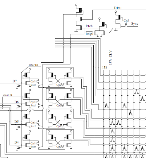
(picture only shows one half of the IR but the other half is identical)
The signal D1x1 is doing all the work. It's also used to control the PC incrementer (although the circuit for that doesn't look quite right to me)
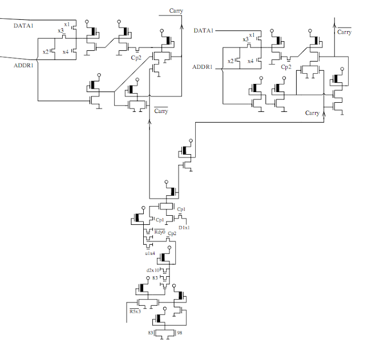
D1x1 is the output of this little collection:
and you see PLA output 83 is one of the inputs, also Clock2 which is one of the six Timing Control signals - the other important ones being IRQ with the I flag, and a composite signal labelling IRQ, NMI, Reset. (Also Rdy0 which is a combination of RnW and RDY and turns up everywhere)
Lo and behold, PLA output 83 detects the 8 branch instructions. So they are treated specially, and deliberately so. Although I still don't quite see why.
(That composite signal is certainly a function of NMI, and I see BRK detection nearby, but I don't see IRQ or RESET, so something isn't quite making sense there.)
Cheers
Ed
thanks for posting such a thorough investigation of this interesting observation. And welcome!
Dr Jefyll wrote:
I believe that the 65xx economizes on silicon by NOT providing specialized hardware to perform the interrupt sequence. Instead, the interrupt is actually an instruction.... Like other instructions, it has a unique op-code that's latched into the chip's Instruction Register when SYNC is high. On subsequent cycles the internal PLA pulls whatever strings and levers are required to get the job done. This approach avoids the cost of adding a complex sequencing mechanism solely to implement interrupts.
Here's the logic which clears the IR - as you suspect, it uses SYNC as a qualifier:
(picture only shows one half of the IR but the other half is identical)
The signal D1x1 is doing all the work. It's also used to control the PC incrementer (although the circuit for that doesn't look quite right to me)
D1x1 is the output of this little collection:
and you see PLA output 83 is one of the inputs, also Clock2 which is one of the six Timing Control signals - the other important ones being IRQ with the I flag, and a composite signal labelling IRQ, NMI, Reset. (Also Rdy0 which is a combination of RnW and RDY and turns up everywhere)
Lo and behold, PLA output 83 detects the 8 branch instructions. So they are treated specially, and deliberately so. Although I still don't quite see why.
(That composite signal is certainly a function of NMI, and I see BRK detection nearby, but I don't see IRQ or RESET, so something isn't quite making sense there.)
Cheers
Ed

Re: A taken branch delays interrupt handling by one instruct
BigEd wrote:
To add to your ideas, Jeff, I had another look at Beregnyei's giant schematic
Here's the logic which clears the IR - as you suspect, it uses SYNC as a qualifier
Here's the logic which clears the IR - as you suspect, it uses SYNC as a qualifier
BigEd wrote:
D1x1 is the output of this little collection:
Quote:
The signal D1x1 [is] used to control the PC incrementer
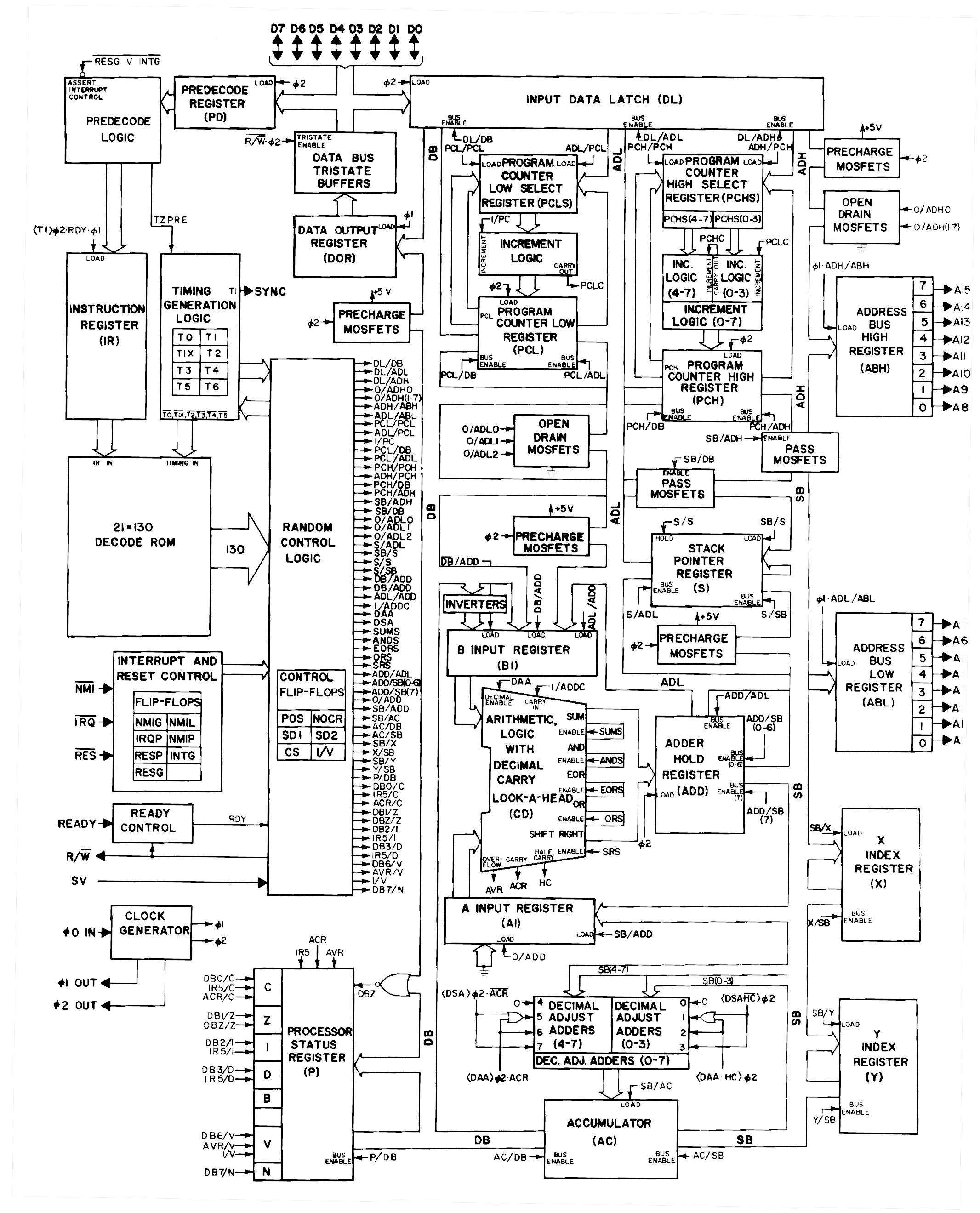
I think the "interrupt as an instruction" theory is amply established. (BTW my insight owes a lot to page A-11, Table A. 5.4 of the MOS Hardware Manual, where they pretty much spill the beans if you're paying attention.) Understanding the interrupt as an instruction shows us its limitations -- why, for example, the Conditional Branch logic might need to take heed. More on that topic some other time, maybe. I don't expect that the '02, the 'C02 and the '816 deal with the matter in exactly the same fashion. And the '816's ABORT introduces yet another flavor! (along with NMI, IRQ, RST and software BRK). Finally:
Quote:
Lo and behold, PLA output 83 detects the 8 branch instructions. So they are treated specially, and deliberately so.
-- Jeff
Re: A taken branch delays interrupt handling by one instruct
Dr Jefyll wrote:
BigEd wrote:
D1x1 is the output of this little collection:
Dr Jefyll wrote:
Quote:
Lo and behold, PLA output 83 detects the 8 branch instructions. So they are treated specially, and deliberately so.
Timing Control looks like it has 5 bits of state(#). There's Clock1 as a signal related to Sync(*), and Clock2 is 1 cycle delayed version, subject to RDY.
And then there's a 4-bit shift register starting at SYNC and subject to RDY. The two Clock signals and the 4 shift register signals go into the PLA. The block diagram would have these signals as T0, T1X, T2, T3, T4, T5. (It has T1 as Sync but T1X to the PLA.) I think there's a subtlety here.
(#) Hmm, but the hardware ref manual mentions 7 states, T0 to T6, for instructions such as ABS,X and BRK.
(*) actually Sync0 which is perhaps an early version of Sync? Is this perhaps valid in the cycle before Sync??
Now, if only we had something more accurate and interactive than the giant schematic (wonderfully useful and interesting though it is)
Eureka! With a transistor-level simulation of the 6502 in hand, we can see exactly what's going on cycle by cycle. (Or even phase by phase.) Huge thanks to Greg James, Barry Silverman and Brian Silverman for their Visual6502 project (website under construction - see other thread) which provided the simulator and the netlist.
Here's a late interrupt into a taken branch, should be timed the same as the example above:
Here's a trace of the simulator's test program:
Now we know exactly what happens, we just need to figure out why! And we can trace any signal on the chip, so long as we can find it. (We can also add and remove transistors if that seems appealling. There are only 3510 transistors there - all the pullups are modelled separately.)
My current thinking is that the succession of Tstates for a normal instruction stream visits 101111 in the last cycle of an instruction, and this is when the interrupt handler kicks off. Taken branches never visit 101111 - they sort of interrupt themselves - and so they wouldn't be interruptible if it weren't for the special handling.
We can see that an interrupt acts differently by watching the Tstates as an interrupt is taken - we don't visit 011111
followed here by another which crosses a page boundary:
in which case the branch does visit the final state 101111 and the next instruction does start with a 011111 as usual.
A branch may be a case a bit like an indexed write where the final instruction state must be reserved in case a page is crossed. In the case of a branch, the next instruction isn't known to have started until it's known that there's no page crossing. The following instruction after a taken branch doesn't have a normal first cycle. And so a taken branch doesn't have a 'final' state, and so it wouldn't be interruptible. Instead it begins the interrupt handler during T2, which means the NMI needs to enter the chip a bit earlier than the usual case in order to catch the window. We see that the other way around: the interrupt appears to have been deferred.
Hope this makes some degree of sense!
Cheers
Ed
Here's a late interrupt into a taken branch, should be timed the same as the example above:
Code: Select all
testNMI(28)
 cyc:10 cp1:1 cp2:0 Add:2304 D:b0 RnW:1  PC:2304 SP:fd  Sync:1 NMI:1  IR:b0 TCstate:111111  fetch:0 clearIR:1 D1x1:1
 cyc:10 cp1:0 cp2:1 Add:2304 D:b0 RnW:1  PC:2304 SP:fd  Sync:1 NMI:1  IR:b0 TCstate:111111  fetch:1 clearIR:0 D1x1:1
 cyc:11 cp1:1 cp2:0 Add:2305 D:fe RnW:1  PC:2305 SP:fd  Sync:0 NMI:1  IR:b0 TCstate:110111  fetch:1 clearIR:0 D1x1:1
 cyc:11 cp1:0 cp2:1 Add:2305 D:fe RnW:1  PC:2305 SP:fd  Sync:0 NMI:1  IR:b0 TCstate:110111  fetch:0 clearIR:1 D1x1:1
 cyc:12 cp1:1 cp2:0 Add:2306 D:00 RnW:1  PC:2306 SP:fd  Sync:0 NMI:1  IR:b0 TCstate:111011  fetch:0 clearIR:1 D1x1:1
 cyc:12 cp1:0 cp2:1 Add:2306 D:00 RnW:1  PC:2306 SP:fd  Sync:0 NMI:1  IR:b0 TCstate:111011  fetch:0 clearIR:1 D1x1:1
 cyc:13 cp1:1 cp2:0 Add:2304 D:b0 RnW:1  PC:2304 SP:fd  Sync:1 NMI:1  IR:b0 TCstate:111111  fetch:0 clearIR:1 D1x1:1
 cyc:13 cp1:0 cp2:1 Add:2304 D:b0 RnW:1  PC:2304 SP:fd  Sync:1 NMI:1  IR:b0 TCstate:111111  fetch:1 clearIR:0 D1x1:1
 cyc:14 cp1:1 cp2:0 Add:2305 D:fe RnW:1  PC:2305 SP:fd  Sync:0 NMI:1  IR:b0 TCstate:110111  fetch:1 clearIR:0 D1x1:1
 cyc:14 cp1:1 cp2:0 Add:2305 D:fe RnW:1  PC:2305 SP:fd  Sync:0 NMI:0  IR:b0 TCstate:110111  fetch:1 clearIR:0 D1x1:1
 cyc:14 cp1:0 cp2:1 Add:2305 D:fe RnW:1  PC:2305 SP:fd  Sync:0 NMI:0  IR:b0 TCstate:110111  fetch:0 clearIR:1 D1x1:1
 cyc:15 cp1:1 cp2:0 Add:2306 D:00 RnW:1  PC:2306 SP:fd  Sync:0 NMI:0  IR:b0 TCstate:111011  fetch:0 clearIR:1 D1x1:1
 cyc:15 cp1:0 cp2:1 Add:2306 D:00 RnW:1  PC:2306 SP:fd  Sync:0 NMI:0  IR:b0 TCstate:111011  fetch:0 clearIR:1 D1x1:1
 cyc:16 cp1:1 cp2:0 Add:2304 D:b0 RnW:1  PC:2304 SP:fd  Sync:1 NMI:0  IR:b0 TCstate:111111  fetch:0 clearIR:1 D1x1:1
 cyc:16 cp1:0 cp2:1 Add:2304 D:b0 RnW:1  PC:2304 SP:fd  Sync:1 NMI:0  IR:b0 TCstate:111111  fetch:1 clearIR:0 D1x1:1
 cyc:17 cp1:1 cp2:0 Add:2305 D:fe RnW:1  PC:2305 SP:fd  Sync:0 NMI:0  IR:b0 TCstate:110111  fetch:1 clearIR:0 D1x1:1
 cyc:17 cp1:0 cp2:1 Add:2305 D:fe RnW:1  PC:2305 SP:fd  Sync:0 NMI:0  IR:b0 TCstate:110111  fetch:0 clearIR:1 D1x1:0
 cyc:18 cp1:1 cp2:0 Add:2306 D:00 RnW:1  PC:2306 SP:fd  Sync:0 NMI:0  IR:b0 TCstate:111011  fetch:0 clearIR:1 D1x1:0
 cyc:18 cp1:1 cp2:0 Add:2306 D:00 RnW:1  PC:2306 SP:fd  Sync:0 NMI:1  IR:b0 TCstate:111011  fetch:0 clearIR:1 D1x1:0
 cyc:18 cp1:0 cp2:1 Add:2306 D:00 RnW:1  PC:2306 SP:fd  Sync:0 NMI:1  IR:b0 TCstate:111011  fetch:0 clearIR:1 D1x1:0
 cyc:19 cp1:1 cp2:0 Add:2304 D:b0 RnW:1  PC:2304 SP:fd  Sync:1 NMI:1  IR:b0 TCstate:111111  fetch:0 clearIR:1 D1x1:0
 cyc:19 cp1:0 cp2:1 Add:2304 D:b0 RnW:1  PC:2304 SP:fd  Sync:1 NMI:1  IR:b0 TCstate:111111  fetch:1 clearIR:1 D1x1:0
 cyc:20 cp1:1 cp2:0 Add:2304 D:b0 RnW:1  PC:2304 SP:fd  Sync:0 NMI:1  IR:00 TCstate:110111  fetch:1 clearIR:1 D1x1:0
 cyc:20 cp1:0 cp2:1 Add:2304 D:b0 RnW:1  PC:2304 SP:fd  Sync:0 NMI:1  IR:00 TCstate:110111  fetch:0 clearIR:1 D1x1:0
 cyc:21 cp1:1 cp2:0 Add:01fd D:b0 RnW:0  PC:2304 SP:fd  Sync:0 NMI:1  IR:00 TCstate:111011  fetch:0 clearIR:1 D1x1:0
 cyc:21 cp1:0 cp2:1 Add:01fd D:23 RnW:0  PC:2304 SP:fd  Sync:0 NMI:1  IR:00 TCstate:111011  fetch:0 clearIR:1 D1x1:0
Code: Select all
 cyc:2 cp1:1 cp2:0 Add:0000 D:a9 RnW:1  PC:0000 SP:fd  Sync:1 NMI:1  IR:00 TCstate:011111  fetch:0 clearIR:1 D1x1:1
 cyc:2 cp1:0 cp2:1 Add:0000 D:a9 RnW:1  PC:0000 SP:fd  Sync:1 NMI:1  IR:00 TCstate:011111  fetch:1 clearIR:0 D1x1:1
 cyc:3 cp1:1 cp2:0 Add:0001 D:00 RnW:1  PC:0001 SP:fd  Sync:0 NMI:1  IR:a9 TCstate:100111  fetch:1 clearIR:0 D1x1:1
 cyc:3 cp1:0 cp2:1 Add:0001 D:00 RnW:1  PC:0001 SP:fd  Sync:0 NMI:1  IR:a9 TCstate:100111  fetch:0 clearIR:1 D1x1:1
 cyc:4 cp1:1 cp2:0 Add:0002 D:20 RnW:1  PC:0002 SP:fd  Sync:1 NMI:1  IR:a9 TCstate:011111  fetch:0 clearIR:1 D1x1:1
 cyc:4 cp1:0 cp2:1 Add:0002 D:20 RnW:1  PC:0002 SP:fd  Sync:1 NMI:1  IR:a9 TCstate:011111  fetch:1 clearIR:0 D1x1:1
 cyc:5 cp1:1 cp2:0 Add:0003 D:10 RnW:1  PC:0003 SP:fd  Sync:0 NMI:1  IR:20 TCstate:110111  fetch:1 clearIR:0 D1x1:1
 cyc:5 cp1:0 cp2:1 Add:0003 D:10 RnW:1  PC:0003 SP:fd  Sync:0 NMI:1  IR:20 TCstate:110111  fetch:0 clearIR:1 D1x1:1
 cyc:6 cp1:1 cp2:0 Add:01fd D:00 RnW:1  PC:0004 SP:10  Sync:0 NMI:1  IR:20 TCstate:111011  fetch:0 clearIR:1 D1x1:1
 cyc:6 cp1:0 cp2:1 Add:01fd D:00 RnW:1  PC:0004 SP:10  Sync:0 NMI:1  IR:20 TCstate:111011  fetch:0 clearIR:1 D1x1:1
 cyc:7 cp1:1 cp2:0 Add:01fd D:00 RnW:0  PC:0004 SP:10  Sync:0 NMI:1  IR:20 TCstate:111101  fetch:0 clearIR:1 D1x1:1
 cyc:7 cp1:0 cp2:1 Add:01fd D:00 RnW:0  PC:0004 SP:10  Sync:0 NMI:1  IR:20 TCstate:111101  fetch:0 clearIR:1 D1x1:1
 cyc:8 cp1:1 cp2:0 Add:01fc D:00 RnW:0  PC:0004 SP:10  Sync:0 NMI:1  IR:20 TCstate:111110  fetch:0 clearIR:1 D1x1:1
 cyc:8 cp1:0 cp2:1 Add:01fc D:04 RnW:0  PC:0004 SP:10  Sync:0 NMI:1  IR:20 TCstate:111110  fetch:0 clearIR:1 D1x1:1
 cyc:9 cp1:1 cp2:0 Add:0004 D:00 RnW:1  PC:0004 SP:10  Sync:0 NMI:1  IR:20 TCstate:101111  fetch:0 clearIR:1 D1x1:1
cyc:9 cp1:0 cp2:1 Add:0004 D:00 RnW:1 PC:0004 SP:10 Sync:0 NMI:1 IR:20 TCstate:101111 fetch:0 clearIR:1 D1x1:1My current thinking is that the succession of Tstates for a normal instruction stream visits 101111 in the last cycle of an instruction, and this is when the interrupt handler kicks off. Taken branches never visit 101111 - they sort of interrupt themselves - and so they wouldn't be interruptible if it weren't for the special handling.
We can see that an interrupt acts differently by watching the Tstates as an interrupt is taken - we don't visit 011111
Code: Select all
  cyc:7 cp1:1 cp2:0 Add:2306 D:b0 RnW:1  PC:2306 SP:fd  Sync:1 NMI:1  IR:4c TCstate:011111  fetch:0 clearIR:1 D1x1:1
  cyc:7 cp1:0 cp2:1 Add:2306 D:b0 RnW:1  PC:2306 SP:fd  Sync:1 NMI:1  IR:4c TCstate:011111  fetch:1 clearIR:0 D1x1:1
  cyc:8 cp1:1 cp2:0 Add:2307 D:01 RnW:1  PC:2307 SP:fd  Sync:0 NMI:1  IR:b0 TCstate:110111  fetch:1 clearIR:0 D1x1:1
  cyc:8 cp1:0 cp2:1 Add:2307 D:01 RnW:1  PC:2307 SP:fd  Sync:0 NMI:1  IR:b0 TCstate:110111  fetch:0 clearIR:1 D1x1:1
  cyc:9 cp1:1 cp2:0 Add:2308 D:00 RnW:1  PC:2308 SP:fd  Sync:0 NMI:1  IR:b0 TCstate:111011  fetch:0 clearIR:1 D1x1:1
  cyc:9 cp1:0 cp2:1 Add:2308 D:00 RnW:1  PC:2308 SP:fd  Sync:0 NMI:1  IR:b0 TCstate:111011  fetch:0 clearIR:1 D1x1:1
 cyc:10 cp1:1 cp2:0 Add:2309 D:a9 RnW:1  PC:2309 SP:fd  Sync:1 NMI:1  IR:b0 TCstate:111111  fetch:0 clearIR:1 D1x1:1
 cyc:10 cp1:0 cp2:1 Add:2309 D:a9 RnW:1  PC:2309 SP:fd  Sync:1 NMI:1  IR:b0 TCstate:111111  fetch:1 clearIR:0 D1x1:1
 cyc:11 cp1:1 cp2:0 Add:230a D:de RnW:1  PC:230a SP:fd  Sync:0 NMI:1  IR:a9 TCstate:100111  fetch:1 clearIR:0 D1x1:1
 cyc:11 cp1:0 cp2:1 Add:230a D:de RnW:1  PC:230a SP:fd  Sync:0 NMI:1  IR:a9 TCstate:100111  fetch:0 clearIR:1 D1x1:1
Code: Select all
 cyc:12 cp1:1 cp2:0 Add:230b D:b0 RnW:1  PC:230b SP:fd  Sync:1 NMI:1  IR:a9 TCstate:011111  fetch:0 clearIR:1 D1x1:1
 cyc:12 cp1:0 cp2:1 Add:230b D:b0 RnW:1  PC:230b SP:fd  Sync:1 NMI:1  IR:a9 TCstate:011111  fetch:1 clearIR:0 D1x1:1
 cyc:13 cp1:1 cp2:0 Add:230c D:f2 RnW:1  PC:230c SP:fd  Sync:0 NMI:1  IR:b0 TCstate:110111  fetch:1 clearIR:0 D1x1:1
 cyc:13 cp1:0 cp2:1 Add:230c D:f2 RnW:1  PC:230c SP:fd  Sync:0 NMI:1  IR:b0 TCstate:110111  fetch:0 clearIR:1 D1x1:1
 cyc:14 cp1:1 cp2:0 Add:230d D:00 RnW:1  PC:230d SP:fd  Sync:0 NMI:1  IR:b0 TCstate:111011  fetch:0 clearIR:1 D1x1:1
 cyc:14 cp1:0 cp2:1 Add:230d D:00 RnW:1  PC:230d SP:fd  Sync:0 NMI:1  IR:b0 TCstate:111011  fetch:0 clearIR:1 D1x1:1
 cyc:15 cp1:1 cp2:0 Add:23ff D:00 RnW:1  PC:23ff SP:fd  Sync:0 NMI:1  IR:b0 TCstate:101111  fetch:0 clearIR:1 D1x1:1
 cyc:15 cp1:0 cp2:1 Add:23ff D:00 RnW:1  PC:23ff SP:fd  Sync:0 NMI:1  IR:b0 TCstate:101111  fetch:0 clearIR:1 D1x1:1
 cyc:16 cp1:1 cp2:0 Add:22ff D:38 RnW:1  PC:22ff SP:fd  Sync:1 NMI:1  IR:b0 TCstate:011111  fetch:0 clearIR:1 D1x1:1
 cyc:16 cp1:0 cp2:1 Add:22ff D:38 RnW:1  PC:22ff SP:fd  Sync:1 NMI:1  IR:b0 TCstate:011111  fetch:1 clearIR:0 D1x1:1
A branch may be a case a bit like an indexed write where the final instruction state must be reserved in case a page is crossed. In the case of a branch, the next instruction isn't known to have started until it's known that there's no page crossing. The following instruction after a taken branch doesn't have a normal first cycle. And so a taken branch doesn't have a 'final' state, and so it wouldn't be interruptible. Instead it begins the interrupt handler during T2, which means the NMI needs to enter the chip a bit earlier than the usual case in order to catch the window. We see that the other way around: the interrupt appears to have been deferred.
Hope this makes some degree of sense!
Cheers
Ed
Re: A taken branch delays interrupt handling by one instruct
HiassofT wrote:
BigDumbDinosaur wrote:
After reading your analysis and looking at the logic graphs, I have to wonder if this characteristic was carried over the the 65C02 and 65816. As you say, it appears to be harmless, but does have some perceptible effect on interrupt latency.
So I need to build an adapter board for my 800XL first...
But, good news is: a friend is sending me some other CPUs to test with, a Rockwell 65C02, a CMD 65SC02 and a 65816. My 2 MHz 65C02 seems to have gone missing during the years, but I pulled a Rockwell 65C02 4 MHz from another board I had completely forgotten about :-)
so long,
Hias
Hi Ed!
Wow, this is really awesome!
Did you get a pre-release of their software? I checked visual6502.org but couldn't find anything except for the static pic yet.
Thanks a lot for the tests and for your analysis! And, at least to me, this makes some sense :-)
so long,
Hias
BigEd wrote:
Eureka! With a transistor-level simulation of the 6502 in hand, we can see exactly what's going on cycle by cycle. (Or even phase by phase.) Huge thanks to Greg James, Barry Silverman and Brian Silverman for their Visual6502 project (website under construction - see other thread) which provided the simulator and the netlist.
Did you get a pre-release of their software? I checked visual6502.org but couldn't find anything except for the static pic yet.
Quote:
And so a taken branch doesn't have a 'final' state, and so it wouldn't be interruptible. Instead it begins the interrupt handler during T2, which means the NMI needs to enter the chip a bit earlier than the usual case in order to catch the window. We see that the other way around: the interrupt appears to have been deferred.
Hope this makes some degree of sense!
Hope this makes some degree of sense!
so long,
Hias
HiassofT wrote:
Did you get a pre-release of their software? I checked visual6502.org but couldn't find anything except for the static pic yet.
Quote:
Thanks a lot for the tests and for your analysis! And, at least to me, this makes some sense :-)
BigEd wrote:
Eureka! With a transistor-level simulation of the 6502 in hand, we can see exactly what's going on cycle by cycle. (Or even phase by phase.)
Code: Select all
cyc:10 cp1:1 cp2:0 Add:2304 D:b0 RnW:1 PC:2304 SP:fd Sync:1 NMI:1 IR:b0 TCstate:111111 fetch:0 clearIR:1 D1x1:1
- How does one interpret the TCstate columns? Do these six-digit binary values correspond to the six timing lines feeding the PLA? Which is which?
What is the signal fetch?
Do clearIR and D1x1 correspond to the signals we were discussing from the schematic (reverse-engineered in previous research)? Apparently you have cross-referenced the old work with the new -- presumably by geographically locating specific circuit features in both contexts!
-- Jeff
Hi Jeff
yes, the forum's line-wrapping is a bit of a hindrance.
yes, the three signals at the end are all from Balazs' schematic. I think clearIR has no effect unless fetch is active.
The 6 TCState lines are indeed the PLA 'timing' inputs - the last four are conventionally labelled T2-T5 I think, and the first two are sync-related. The first would conventionally be called T0 but doesn't precisely correspond to Sync because of the taken-branch effect. Even if it did correspond to Sync, I think T0 is a misnomer because the active instruction in the IR is still the previous one. The second signal is normally active in the cycle before Sync - not sure what that should be called!
Notice in the traces that these signals aren't quite one-cold: sometimes we visit 111111 and sometimes 100111.
I completely agree that this is going to take a bit of digesting!
It would be good to run a set of LDA and STA in all addressing modes, and with page crossings where applicable. But even then, interactions with the previous instruction could be interesting.
(I don't think I've yet traced an indirect or indexed addressing mode - there's no disassembly so I'm not sure.)
It would be interesting to see if this specific chip - a revision D - has the famous ROR bug.
Cheers
Ed