6502.org Forum  Projects  Code  Documents  Tools  Forum
It is currently Sat Nov 16, 2024 5:04 pm

All times are UTC


Post new topic Reply to topic  [ 103 posts ]  Go to page Previous  1, 2, 3, 4, 5, 6, 7  Next
Author Message
 Post subject:
PostPosted: Sat Jan 09, 2010 10:03 pm 
Offline
User avatar

Joined: Thu May 28, 2009 9:46 pm
Posts: 8491
Location: Midwestern USA
GARTHWILSON wrote:
I hate to persist, but there are too many problems with BDD's post to just let it go.

Quote:
Therefore, the addressed device ***MUST*** stay open for access until tDHR has expired. There's no sure way to guarantee this if addressing is qualified by Ø2 as you are doing. In your design, as soon as Ø2 falls, your chip decode will become invalid, chip select will be deasserted following gate delays (very short with 74AC logic), and in the case of the SRAM, it is not likely you will meet the tDHR timing requirement. Ergo there won't be any data to read.

False, for two reasons. For one, his glue logic takes most of that 10ns, and for another, bus capacitance will easily hold the data for the rest of the time, as nothing else is driving the data bus yet. The small CMOS leakage along with the capacitive loading on the lines would hold the logic state for a good dozen microseconds (and possibly much longer) if you were to stop the clock immediately after phase 2 goes down.

I'll respond to that with a story.

In the 1950s, the U.S. Air Force was using modified F104s to give pilots an opportunity to experience travel into low space without resorting to the use of full-blown rocket flight. The F104s were equipped with hydrogen peroxide catalyst rockets to propel the plane to altitudes exceeding 100,000 feet, a region in which the plane's J79 engine would, of course, be useless. HP thrusters were fitted to the wingtips for control as the plane left the atmosphere.

Gen. Chuck Yeager was involved with this program and, in fact, was largely responsible for working out the flight procedure. During a test flight in which he ascended to about 104,000 feet, he got into a situation that almost killed him, in part due to trying to take advantage of an undefined behavior of the F104.

The procedure was to climb to about 70,000 feet on jet power, fire the rockets to continue the ascent and shut down the J79 to prevent "hot section" damage due to insufficient intake air. After passing through the apex of the climb, the plane would be put into a (hopefully) controlled descent, using the rockets and wingtip thrusters to pitch the plane down. This action would bring it back into the atmosphere, at which time air rushing through the J79 would windmill the turbine ("spool") assembly and permit an engine restart.

Parenthetical note: the F104's controls were dependent on hydraulic pressure derived from a pump driven from the spool. If the spool wasn't turning, neither was the pump, and the pilot had no control to speak of. Therefore, getting the engine running during the descent was paramount. Alternatively, if unable to actually fire the engine during descent, the pilot could continue down to keep the spool windmilling so control could be maintained for a dead stick landing.

Anyhow, after passing through the apex of his climb, Gen. Yeager headed back down. Unfortunately, as the F104 got back into more solid air it went into a flat spin due to its tendency to pitch up during steep descent angles. Under normal conditions, Yeager would have had little difficulty in counteracting this behavior and getting out of the spin. However, he had no flight controls because the J79 wasn't running and, adding insult to injury, the spool wasn't windmilling, since in the spin, insufficient air was being rammed into the engine. Ergo he didn't have the ability to break the spin, and down he went, completely out of control.

At 30,000 feet, with the spin worsening, Yeager decided he would deploy the plane's drag 'chute to get the nose down and regain control. The 'chute was intended to assist in slowing the plane after landing—the F104's wing design required high takeoff and landing speeds. However, the 'chute's and the plane's behavior in flight was not quantified by the machine's builder. Yeager, of course, knew this but assumed the 'chute's drag immediately after deployment would force the nose down and get him out of the spin.

It didn't work that way. The 'chute deployed, momentarily forced the nose down, but then separated from the plane due to his airspeed being too high. The F104 promptly pitched up and went back into the flat spin. His efforts to save the specially equipped plane had failed and he (barely) ejected in time to save himself. The general was seriously burned, almost permanently lost vision, and had narrowly escaped death. The plane, of course, ended up punching a big hole in the ground.

My point is this: assuming that an undefined behavior of something will work to your advantage is fallacy. Assuming a circuit will behave in a predictable fashion due to the effects of an unquantified (in most designs) phenomenon like stray capacitance is fallacy. You might get away with it some or most of the time, but not always.
Quote:
Quote:
During a write cycle, you will have another circuit bug. As I said above, the data bus is never valid when Ø2 is low. If you directly connect the SRAM's /WE input to the MPU's R/W output, you will be telling the SRAM to accept data (assuming a write cycle) while Ø2 is low, a period during which the MPU is fiddling with the address lines. At higher clock speeds, it's very likely the SRAM may react to /WE while the address bus is in transition. The result is the invalid data on the data bus will be written to an invalid address in the SRAM.

No again, because the select logic does not have the RAM selected during the phase-2-low period. You're saying it cannot work, but the fact is that it has worked perfectly 100% of the time for all 16 years in the field in our products where the R/W\ line goes directly to the SRAM with no phase-2 qualification. Of the very few computer problems we've had, they've all been due to bad connections.

Ah, you're metaphorically putting words in my mouth. I did not say it "cannot work." I said, in so many words, the potential was there for it to not work due to A0-A15 not being fully settled until near the end of Ø2 low and the addressed device possibly getting a wrong address for a short period of time while R/W is asserted. Qualifying R/W with Ø2 high eliminates that possibility.

_________________
x86?  We ain't got no x86.  We don't NEED no stinking x86!


Top
 Profile  
Reply with quote  
 Post subject:
PostPosted: Sat Jan 09, 2010 10:23 pm 
Offline
User avatar

Joined: Fri Aug 30, 2002 1:09 am
Posts: 8541
Location: Southern California
Quote:
My point is this: assuming that an undefined behavior of something will work to your advantage is fallacy. Assuming a circuit will behave in a predictable fashion due to the effects of an unquantified (in most designs) phenomenon like stray capacitance is fallacy. You might get away with it some or most of the time, but not always.

Good story, but capacitance holding information in a charge is what makes DRAM work, 100% reliably. (Just make sure all the loads on the bus are CMOS, so they don't require any current.) If there's anything else driving the bus at that time, then you'll have bus contention anyway, meaning you'll have other problems.

Actually, one of our forum members called WDC years ago to ask about the same kind of thing where the data sheet did not guarantee the write data to be valid very long after phase 2 falls. It looked scary short. The engineer he talked to said that the data sheet was full of baloney there and that in real-world conditions, the data would persist until the bus is driven the next time.

Quote:
the potential was there for it to not work due to A0-A15 not being fully settled until near the end of Ø2 low and the addressed device possibly getting a wrong address for a short period of time while R/W is asserted. Qualifying R/W with Ø2 high eliminates that possibility.

As he's qualifying the chip select with phase 2 (not the fastest, but it works), there is no potential at all for erroneous writes when phase 2 is low.


Last edited by GARTHWILSON on Sat Jan 09, 2010 10:32 pm, edited 2 times in total.

Top
 Profile  
Reply with quote  
 Post subject:
PostPosted: Sat Jan 09, 2010 10:28 pm 
Offline
User avatar

Joined: Fri Aug 30, 2002 1:09 am
Posts: 8541
Location: Southern California
Quote:
Quote:
...I just put a couple of oscilloscope probes on my workbench computer which has a 65802, and the address does come out soon after phase 2 falls. But according to the data sheet for the 65c02 (I can't find my data sheet for the '802), it's quite different. It shows that as you close in on the processor's maximum speed, the soonest time that the address is guaranteed to be valid and stable gets mighty close to the rising edge of phase 2. If that's true, I suspect that a major cause of crashing when you go too fast is that the address is not out in time before phase 2 rises. Daryl, can you check this on your '816 since you just stepped its speed way up? (Or anyone else with any WDC processor running in the teens of MHz.)

OK, got my ancient scope out and this is what I saw.

CH A connected to A0, CH B on the TTL Oscillator output (trigger)

Pulse width confirmed to be 69.8 ns on the clk (14.318 MHz).

A0 begins to change states at 12.5ns from falling edge of clk. It reaches the new state at approximately 26ns. This would infer that the max clock speed for my SBC-3 would be about 19.2 MHz.

The datasheet gives max setup time, tADS, as 30ns.

For those interested in the BANK address setup time, the tBAS spec has a max of 33ns. I measured approx 26ns on that line as well.

Shucks. I was hoping it would be faster. Thanks anyway. It's good to have the info, even if it's not what I had hoped.


Top
 Profile  
Reply with quote  
 Post subject:
PostPosted: Tue Jan 12, 2010 12:30 am 
Offline

Joined: Mon Mar 02, 2009 7:27 pm
Posts: 3258
Location: NC, USA
Ok, so how much time does this leave for address decode logic? I am still finding it difficult to interpret the timing logic. While ABT logic is plenty fast, 2 or more logic units in series adds up quick (~7ns)... I'm looking at using an ATF22V10C-75, which is 7.5ns. At the speeds discussed (~14+MHz), is it worth it to investigate SPLD's from Atmel?

_________________
65Org16:https://github.com/ElEctric-EyE/verilog-6502


Top
 Profile  
Reply with quote  
 Post subject:
PostPosted: Tue Jan 12, 2010 5:23 am 
Offline
User avatar

Joined: Fri Aug 30, 2002 9:02 pm
Posts: 1747
Location: Sacramento, CA
I don't see why not. My CPLD is a 15ns part and it is decoding the address bus, lower 4 bits of the bank address from the data bus, and the R/W, /RES, and PHI2 and creating an I/O select and RAM selects with no trouble at 14MHz on the 65816. It will depend upon several factors, including bus loading and capacitance.

Daryl


Top
 Profile  
Reply with quote  
 Post subject:
PostPosted: Wed Jan 13, 2010 3:35 am 
Offline
User avatar

Joined: Thu May 28, 2009 9:46 pm
Posts: 8491
Location: Midwestern USA
8BIT wrote:
I don't see why not. My CPLD is a 15ns part and it is decoding the address bus, lower 4 bits of the bank address from the data bus, and the R/W, /RES, and PHI2 and creating an I/O select and RAM selects with no trouble at 14MHz on the 65816. It will depend upon several factors, including bus loading and capacitance.

Daryl

And you can get CPLDs with single digit nanosecond performance. For example, the Xilinx XC95108 has, and I quote from the datasheet, "7.5 ns pin-to-pin logic delays on all pins." Should be fast enough, I'd think. :)

BTW, the XC95108 is available in a PLCC84 package with mucho I/O pins. Order part number XC95108-7PCG84C.

_________________
x86?  We ain't got no x86.  We don't NEED no stinking x86!


Top
 Profile  
Reply with quote  
 Post subject:
PostPosted: Thu Jan 14, 2010 5:36 am 
Offline

Joined: Mon Mar 02, 2009 7:27 pm
Posts: 3258
Location: NC, USA
BigDumbDinosaur wrote:
...And you can get CPLDs with single digit nanosecond performance. For example, the Xilinx XC95108 has, and I quote from the datasheet, "7.5 ns pin-to-pin logic delays on all pins." Should be fast enough, I'd think. :)

BTW, the XC95108 is available in a PLCC84 package with mucho I/O pins. Order part number XC95108-7PCG84C.


I plan to start with the Atmel ATF22V10C only because my EEPROM G540 burner, (which I am presently using to program the 8Kx8 Atmel AT28HC64B-70PL EEPROM), also burns .jedec files for the EESPLD 22V10 series. They have versions that go down to 5ns. I've been able to buy a few Atmel 7.5ns for a little over $3 each.

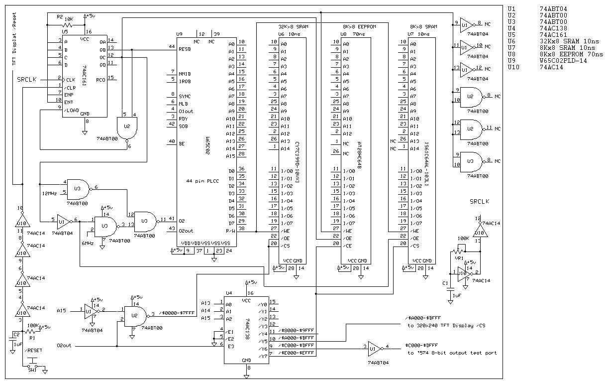
BUT first, tomorrow the digikey order comes in for some 'ABT IC's, 74AC14, and 74AC161, and I put my idea to test. Final schematic below: Thanks to leeeeee, nightmaretony, Garth for the high spead MUX circuit for phase2, and BDD and 8BIT for their time spent on critique and advice. I'll wire it all up after next weekend. Hopefully have an unwirewrap tool by then...

Instead of editing/re-editing 1 or 2 old posted schematics, I chose to keep the old and post new, to show the progression...

Hope it works, or this thread should die real quick ;).

Image

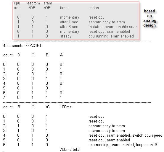
Truth table logic for the counter:
Image

_________________
65Org16:https://github.com/ElEctric-EyE/verilog-6502


Top
 Profile  
Reply with quote  
 Post subject:
PostPosted: Tue Jan 19, 2010 2:01 am 
Offline

Joined: Mon Mar 02, 2009 7:27 pm
Posts: 3258
Location: NC, USA
I wired it all up. Having problems with the SRClk, which is derived from the 74AC14... Unstable frequency on the scope... Tomorrow is another day off. I spent a good 10 hours on rewiring most of the address decoding, including adding 4 IC's. The Schematic above is what I have so far, and is up to date.

_________________
65Org16:https://github.com/ElEctric-EyE/verilog-6502


Top
 Profile  
Reply with quote  
 Post subject:
PostPosted: Tue Jan 19, 2010 9:35 am 
Offline

Joined: Tue Jul 05, 2005 7:08 pm
Posts: 1043
Location: near Heidelberg, Germany
BigDumbDinosaur wrote:
I'll respond to that with a story.


Nice read. I have a story too. When I developed my RAMDisk board (re-using the old 30pin SIMMs) I had a long discussion with Bil Herd, the hardware designer of the Commodore 128. I learned a lot about hardware design, esp. for a production environment. For example they created the machines (in general) without a (timing) spec violation! I.e. no stray capacities used to hold valid data etc.

I think it's an amazing read:
http://www.6502.org/users/andre/icaphw/design.html

André


Top
 Profile  
Reply with quote  
 Post subject:
PostPosted: Tue Jan 19, 2010 7:16 pm 
Offline

Joined: Mon Mar 02, 2009 7:27 pm
Posts: 3258
Location: NC, USA
Fixed the oscillator part. That is just a crappy little oscillator circuit using 1 Schmitt trigger. I had to make one using 3 inverters, no prob there. It is making the 'AC161 count up every 1.5 sec's, giving the software plenty of time to copy. Also, instead of 12MHz, I am using 6 MHz on both NAND gates, since I know it runs reliably at that speed. Not working yet...


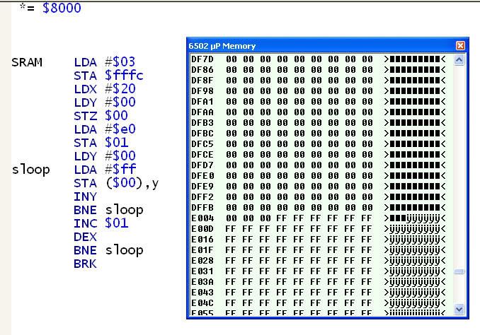
I am writing the portion of code that copies the EEPROM to the RAM, and just to make sure I get all the variables right I made a test program. It's not working like expected. Is there an error in the debugging part of M. Kowalski's assembler?. It should store #$FF from $E000 to $FFFF. For some odd reason it is starting at $E007. Here's a pic of the software and the memory, after the program has been run:

Image

_________________
65Org16:https://github.com/ElEctric-EyE/verilog-6502


Top
 Profile  
Reply with quote  
 Post subject:
PostPosted: Tue Jan 19, 2010 7:45 pm 
Offline

Joined: Sun Sep 15, 2002 10:42 pm
Posts: 214
ElEctric_EyE wrote:
Fixed the oscillator part. That is just a crappy little oscillator circuit using 1 Schmitt trigger. I had to make one using 3 inverters, no prob there. It is making the 'AC161 count up every 1.5 sec's, giving the software plenty of time to copy. Also, instead of 12MHz, I am using 6 MHz on both NAND gates, since I know it runs reliably at that speed. Not working yet...


I am writing the portion of code that copies the EEPROM to the RAM, and just to make sure I get all the variables right I made a test program. It's not working like expected. Is there an error in the debugging part of M. Kowalski's assembler?. It should store #$FF from $E000 to $FFFF. For some odd reason it is starting at $E007. Here's a pic of the software and the memory, after the program has been run:

Image


o You are loading Y with zero twice, probably because you converted the STY to a STZ.

o The inner loop does not need to load the accumulator with $FF every time through the loop, since the accumulator is not modified in the loop.

I don't know why it's starting at $e007 either. I suspect your entry point is wrong somehow.

Toshi


Top
 Profile  
Reply with quote  
 Post subject:
PostPosted: Tue Jan 19, 2010 8:00 pm 
Offline

Joined: Tue Nov 18, 2003 8:41 pm
Posts: 250
fachat wrote:
For example they created the machines (in general) without a (timing) spec violation! I.e. no stray capacities used to hold valid data etc.


It's been some years since I looked at the timing in that detail
but my recollection is that the C64 didn't quite fit in the worst case
at least for some models.

The stray capacitance is presumably built into the timing spec's
in some way. Whether that's typical or worst case I don't know,
but I'd assume it's for (an estimate of) the typical case.

ie the timing may be spec'd worst case but how can they know
how much capacitance you're driving.


Top
 Profile  
Reply with quote  
 Post subject:
PostPosted: Tue Jan 19, 2010 8:22 pm 
Offline
User avatar

Joined: Fri Aug 30, 2002 1:09 am
Posts: 8541
Location: Southern California
I don't see any reason why it would start at E007, but I would do it this way (some explanation is in the comments):
Code:
SRAM    STZ  00           ; Set up addr base lo byte,
        LDA  #$E0         ; then hi byte.
        STA  01

        LDA  #$FF         ; Value to fill RAM with.  Load A only once.
        LDY  #0           ; Init index for small inner loop.
sloop         STA  (0),Y
              INY
           BNE  sloop
           INC  01        ; Outer loop's index is the addr base high byte itself
        BNE  sloop        ; so when it's done filling page FF, it drops through.

        LDA  #03          ; Now fill in the RST vector.  (If you do it first, it gets
        STA  $FFFC        ;   overwritten by the loop above.)
        LDA  ?            ; incl high byte, which was left off earlier.
        STA  $FFFD


Top
 Profile  
Reply with quote  
 Post subject:
PostPosted: Tue Jan 19, 2010 8:47 pm 
Offline
User avatar

Joined: Fri Aug 30, 2002 1:09 am
Posts: 8541
Location: Southern California
Quote:
ie the timing may be spec'd worst case but how can they know
how much capacitance you're driving.

The C64, IIRC, had a lot of LS logic whose inputs require current, and that current will discharge the capacitances. But if you use all CMOS, there's essentially no current (it's guaranteed to not be over 2µA per pin, and that's at a temperature extreme); then no matter how much or how little capacitance you have (it will always be some positive, non-zero amount), an undriven line will hold its logic state. With the 2µA maximum leakage and 5pF normal capacitance per pin, even before including the capacitance of the socket and traces, it will always hold the logic state for at least a microsecond worst case and probably far more. Again that's if everything is CMOS, which I don't think the C64 was. The microsecond is if you only pulled it down to .4V and .8V becomes "no man's land," so it really is worst case. 5pF times (.8-.4)V divided by 2µA equals 1µs or 1000ns.


Top
 Profile  
Reply with quote  
 Post subject:
PostPosted: Tue Jan 19, 2010 9:03 pm 
Offline

Joined: Mon Mar 02, 2009 7:27 pm
Posts: 3258
Location: NC, USA
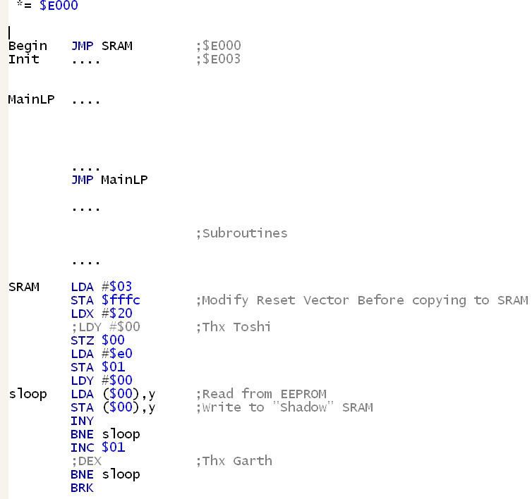
That was just a piece of test software to make sure I get my INC's, and DEX's right so I don't overlap into other memory space accidentally. I'll have to assume the software really is copying, starting at $E000 and not $E007. The "real" software which is on the EEPROM looks like this:

Image

The Reset Vector has already been programmed into the EEPROM for $E000. This piece of code modifies it after booting from the EEPROM to $E003, the CPU will be reset once again by the counter and the EEPROM /OE disabled, and the SRAM /OE enabled, and the Init, and Main Loop will be running from the SRAM at that point. That's the idea anyway.

_________________
65Org16:https://github.com/ElEctric-EyE/verilog-6502


Top
 Profile  
Reply with quote  
Display posts from previous:  Sort by  
Post new topic Reply to topic  [ 103 posts ]  Go to page Previous  1, 2, 3, 4, 5, 6, 7  Next

All times are UTC


Who is online

Users browsing this forum: No registered users and 15 guests


You cannot post new topics in this forum
You cannot reply to topics in this forum
You cannot edit your posts in this forum
You cannot delete your posts in this forum
You cannot post attachments in this forum

Search for:
Jump to: