Gonna have to think about this one guys. I'm intrigued. Gonna try to figure this out. Thanks? heh...
OK, I am understanding. Drawing it now.
Speeding up the 65C02
-
ElEctric_EyE
- Posts: 3260
- Joined: 02 Mar 2009
- Location: OH, USA
-
ElEctric_EyE
- Posts: 3260
- Joined: 02 Mar 2009
- Location: OH, USA
-
ElEctric_EyE
- Posts: 3260
- Joined: 02 Mar 2009
- Location: OH, USA
-
BigDumbDinosaur

- Posts: 9428
- Joined: 28 May 2009
- Location: Midwestern USA (JB Pritzker’s dystopia)
- Contact:
ElEctric_EyE wrote:
BigDumbDinosaur wrote:
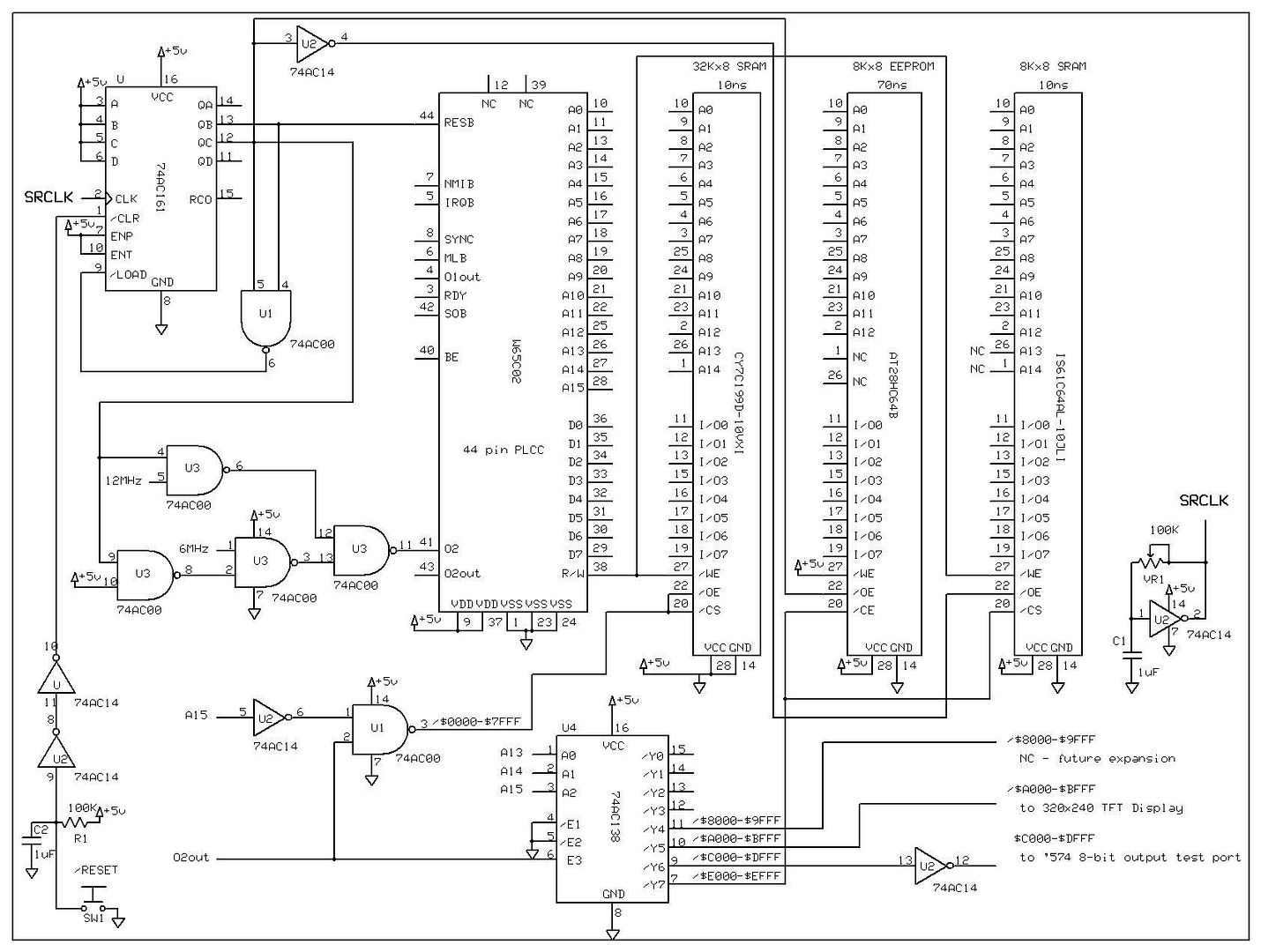
... instead use Ø2 to qualify R/W and hook A15 directly to the SRAM's /CS. SRAM is going to be in anytime the address is less than $8000, so no need for any additional logic in that department. With A15 directly driving /CS, he'd have almost all of Ø2 low to get the address setup done. As soon as Ø2 went high, the SRAM would be ready for read/write. Just an opinion, of course.
You should not be using that method to control address decode. If you do, you lose part of the valid read/write cycle to address setup time, which will set a hard limit on the maximum clock speed. Your decoding methodology should react to A0-A15 as soon as possible and R/W should only get into the picture if a write to a given address is intended to touch a different device than a read to the same address.
If you examine the 65C02 timing diagram, you'll see that R/W becomes valid before the rise of Ø2. If you want to read from a device at address X but not write to it, you'd qualify the chip select (/CS) for that device with R/W:
Code: Select all
/CS = X & !R/WA write to a different device at the same address would be:
Code: Select all
/CS = X & R/W
Last edited by BigDumbDinosaur on Wed Jan 06, 2010 5:51 am, edited 1 time in total.
x86? We ain't got no x86. We don't NEED no stinking x86!
-
Nightmaretony
- In Memoriam
- Posts: 618
- Joined: 27 Jun 2003
- Location: Meadowbrook
- Contact:
also, all your enable pins pulled up high, you want to have them go through a 1k or 4.7k pullup resistor. we had that mistake in an arcade game and it blew out the sprite control on a fairly constant basis. (Sky shark, if you wonder which)....
"My biggest dream in life? Building black plywood Habitrails"
-
ElEctric_EyE
- Posts: 3260
- Joined: 02 Mar 2009
- Location: OH, USA
-
GARTHWILSON

- Forum Moderator
- Posts: 8774
- Joined: 30 Aug 2002
- Location: Southern California
- Contact:
It's not to AND the two frequencies together, but you use the AND gates so when the gate taking in the unwanted signal has one of its inputs low, there's no AC output from that gate. The output is at a DC high however so the final AND gate passes the frequency through from the other one. IOW, you're using it as a selector switch.
-
BigDumbDinosaur
- Posts: 9428
- Joined: 28 May 2009
- Location: Midwestern USA (JB Pritzker’s dystopia)
- Contact:
ElEctric_EyE wrote:
I am really confused now... Did I draw the last schematic wrong?..... PM^
Forget about the clock frequency for a minute and focus on the selection of RAM, ROM, etc. ROM is a read-only device, therefore the only time when it would make sense to select it would be when the 65C02's R/W line is high (read mode). So, to select the ROM your logic would be the inverted logical AND of R/W and the address bits on which the ROM is visible. That is, your decoding circuitry would include a NAND of R/W so the ROM's /CS (chip select) input is low only when R/W is high and the ROM has been addressed by the MPU.
Conversely, the RAM that appears at the same address as the ROM would be selected only when a valid address is on the bus AND R/W is low.
Now, here's where it gets sticky. Your goal, as I understand it, is to at reset copy the ROM to RAM at the same address, completely map out the ROM and run from RAM. So the circuit at reset must obey the logic I described above: ROM access on read cycles, RAM access on write cycles. Simple enough.
However, once the ROM dump into RAM has finished, your circuit has to completely disable ROM and write-protect the RAM by guaranteeing that the RAM's /WE line cannot ever be brought low following the ROM dump. Otherwise, a wild write due to a program bug will scribble on the RAM, boogering up your code and most likely crashing the machine. You circuit has the /WE input of the SRAM at $E000 hooked directly to the MPU's R/W line. Therefore, the RAM is not write-protected, as the device you are using ignores /OE when /WE is asserted.
Another possible error I see in your circuit is in the use of Ø2 to qualify device selection. In my opinion, that's incorrect. Device selection should be a function of what the MPU places on A0-A15, subject to the R/W qualification I described before. Getting Ø2 mixed in with device selection means the devices only have the high side of Ø2 to react to A0-A15 and get ready for access. That will not work correctly as you crank up the clock speed. You want to select a device without regard to Ø2 low. The MPU will place a valid address on A0-A15 shortly after Ø2 goes low. R/W will go valid about 60 percent of the way through Ø2 low and remain valid until shortly after the next fall of Ø2. Therefore, if you qualify an address with R/W, your device should be set up for access by the time Ø2 goes high. In the case of the SRAM, it'll be ready in plenty of time, even with the MPU running at 14 MHz or better.
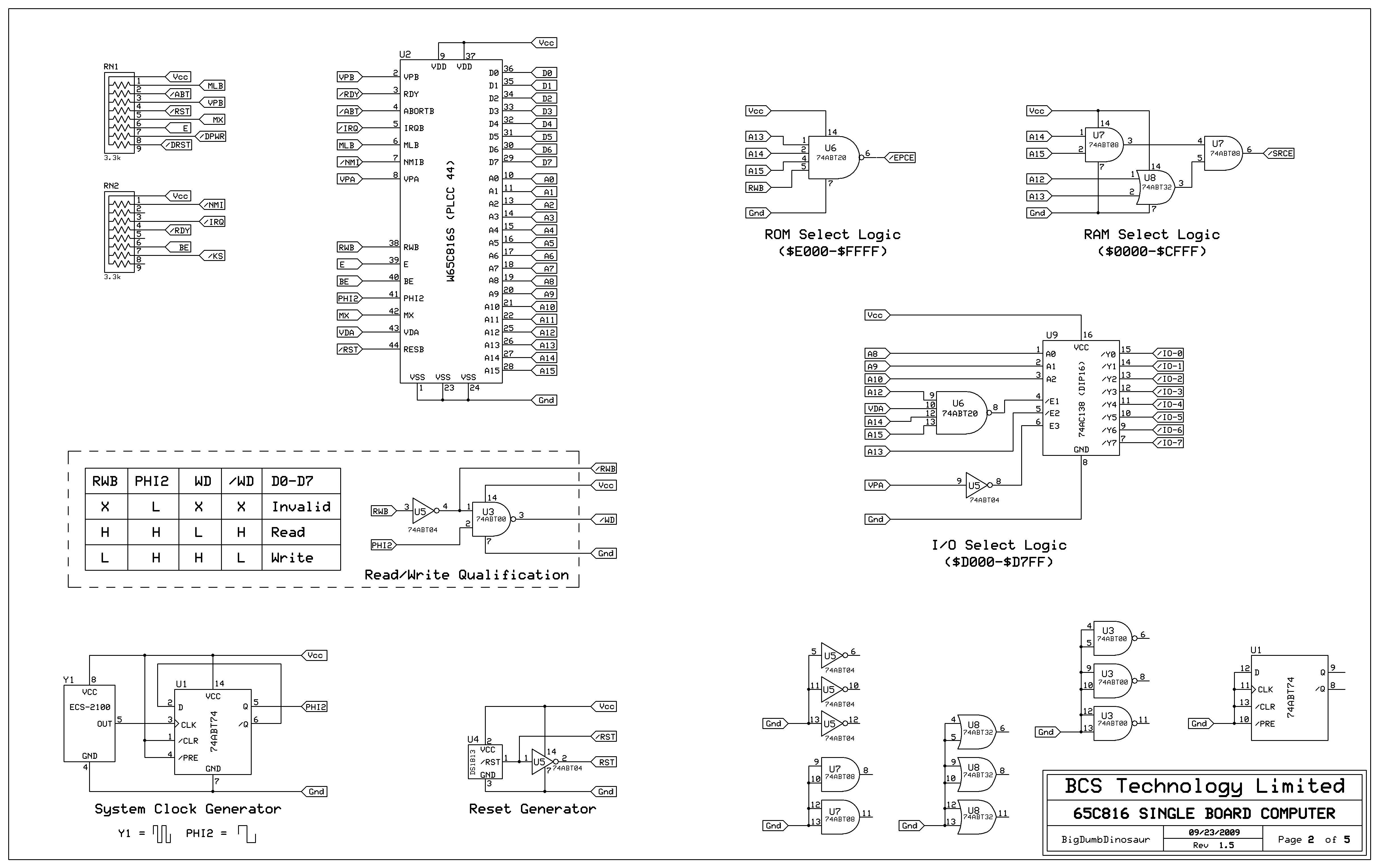
Here's the chip select circuitry for my POC computer. Note how Ø2 has nothing to do with device selection. Also, note that ROM is only selected when RWB (the '816 R/W output) is high. This arrangement has been tested up to 8 MHz.
While on the subject of R/W, all writes should be qualified by Ø2. You should avoid a write operation unless Ø2 is high, as D0-D7 cannot be considered valid unless Ø2 is high. Your circuit uses R/W without regard to the Ø2 timing, which will assuredly cause random errors.
x86? We ain't got no x86. We don't NEED no stinking x86!
-
GARTHWILSON
- Forum Moderator
- Posts: 8774
- Joined: 30 Aug 2002
- Location: Southern California
- Contact:
Quote:
However, once the ROM dump into RAM has finished, your circuit has to completely disable ROM and write-protect the RAM by guaranteeing that the RAM's /WE line cannot ever be brought low following the ROM dump. Otherwise, a wild write due to a program bug will scribble on the RAM, boogering up your code and most likely crashing the machine. You circuit has the /WE input of the SRAM at $E000 hooked directly to the MPU's R/W line. Therefore, the RAM is not write-protected, as the device you are using ignores /OE when /WE is asserted.
Quote:
Another possible error I see in your circuit is in the use of Ø2 to qualify device selection. In my opinion, that's incorrect. Device selection should be a function of what the MPU places on A0-A15, subject to the R/W qualification I described before. Getting Ø2 mixed in with device selection means the devices only have the high side of Ø2 to react to A0-A15 and get ready for access. That will not work correctly as you crank up the clock speed. You want to select a device without regard to Ø2 low. The MPU will place a valid address on A0-A15 shortly after Ø2 goes low.
Quote:
While on the subject of R/W, all writes should be qualified by Ø2. You should avoid a write operation unless Ø2 is high, as D0-D7 cannot be considered valid unless Ø2 is high. Your circuit uses R/W without regard to the Ø2 timing, which will assuredly cause random errors.
http://WilsonMinesCo.com/ lots of 6502 resources
The "second front page" is http://wilsonminesco.com/links.html .
What's an additional VIA among friends, anyhow?
The "second front page" is http://wilsonminesco.com/links.html .
What's an additional VIA among friends, anyhow?
Maybe I'm not following you here
But that's what the chip select does. (no?)
So if you're talking about making sure that there's enough delay
in R/W to track the chip select logic delays, I don't see how just
gating R/W with phi2 guarantees that.
BigDumbDinosaur wrote:
While on the subject of R/W, all writes should be qualified by Ø2. You should avoid a write operation unless Ø2 is high, as D0-D7 cannot be considered valid unless Ø2 is high. Your circuit uses R/W without regard to the Ø2 timing, which will assuredly cause random errors.
So if you're talking about making sure that there's enough delay
in R/W to track the chip select logic delays, I don't see how just
gating R/W with phi2 guarantees that.
-
ElEctric_EyE
- Posts: 3260
- Joined: 02 Mar 2009
- Location: OH, USA
bogax wrote:
...And assuming you're not going to write protect SRAM once it's written (since you don't show that).
GARTHWILSON wrote:
... or if you want self-modifying code (which is justifiable only on rare occasion).
BigDumbDinosaur wrote:
...This sort of logic will select the desired device during the low half of Ø2, shortly after A0-A15 become valid. The device will remain selected through Ø2 high. You wouldn't use Ø2 to qualify any chip selects.
Your qualifying the Read and Writes with Phase2 reminds me of an 8080-style interface I tried with the TFT display, which didn't work (at sub 7MHz speeds, I later found out why and explain later on in the thread). Keep in mind though, I'm not using the 65816. The timing diag's look abit different to me, compared to the 6502.
It's here: (4th post down) viewtopic.php?t=1370&postdays=0&postorder=asc&start=75.
Or here, for the direct link: http://www.atarimagazines.com/computeii ... page17.php

GARTHWILSON wrote:
...I just put a couple of oscilloscope probes on my workbench computer which has a 65802, and the address does come out soon after phase 2 falls. But according to the data sheet for the 65c02 (I can't find my data sheet for the '802), it's quite different. It shows that as you close in on the processor's maximum speed, the soonest time that the address is guaranteed to be valid and stable gets mighty close to the rising edge of phase 2. If that's true, I suspect that a major cause of crashing when you go too fast is that the address is not out in time before phase 2 rises. Daryl, can you check this on your '816 since you just stepped its speed way up? (Or anyone else with any WDC processor running in the teens of MHz.)
Daryl
-
BigDumbDinosaur
- Posts: 9428
- Joined: 28 May 2009
- Location: Midwestern USA (JB Pritzker’s dystopia)
- Contact:
ElEctric_EyE wrote:
...But the old school 6502 MOS manual says that A0-A15 was only valid during phase2 high...The timing diag's look a bit different to me, compared to the 6502.
My opinion, for what it's worth, is that your address decoding methodology is improper. Chips selects should not be qualified by Ø2 at all. Although bus states are dependent on the phase of Ø2, the bus changes do not coincide with the rise and fall of the clock, and that is where I think your circuit is going to have trouble.
The 65xx family has, for all practical purposes, two operating states. One is present while Ø2 is low, which is when the MPU fiddles with A0-A15 and conditions control outputs, such as R/W. During that time, the data bus is invalid. The other state is when Ø2 is high, which is when the data bus becomes valid and a read or write operation can be carried out. Your design is not acknowledging these characteristics of the 'C02 (also true of the '816) and, I believe, is headed toward a timing train wreck.
Consider your SRAM, for example. It has three control inputs: /CS, /OE and /WE. The idealized (read "correct") way to address this part is for /CS to be asserted as soon as any address to which the SRAM is to respond is placed on A0-A15 by the MPU. A0-A15 is guaranteed to be stable no more than tADS nanoseconds after the fall of Ø2, an interval of 30ns maximum on a 'C02 running at 14 MHz. During the time period denoted by tADS, A0-A15 are changing and the address bus is not valid. Add on the gate delays in your glue logic and just about all of Ø2 low will be used up in address setup. Keep in mind that the SRAM itself will have some delay after selected before its internal logic produces the correct row/column address.
Of course, the SRAM has to know whether it is to be read or written. A read operation can be qualified by inverting the MPU's R/W output and applying the output of the inverter to /OE. According to the timing diagram, R/W also becomes valid at tADS. Therefore, assuming a clock rate of 14 MHz, the needed SRAM setup will occur no more than 30ns plus gate delays after the fall of Ø2 and, if you are using 12-15ns SRAM, the part should be ready for business by the time the MPU gets around to accessing D0-D7.
Depending on the SRAM, you may be able to dispense with qualifying /OE and may be able to simply tie it to /CS. In other cases, that arrangement could be ambiguous during a write cycle, causing difficult to diagnose conditions. You need to carefully read the narrative for the SRAM you are using to verify that asserting /OE during a write operation is an acceptable procedure. If not, you must qualify it with an inverted R/W signal.
Now, here comes the important part. The MPU does not access D0-D7 until well after the rise of Ø2. In a read cycle, the MPU doesn't sample D0-D7 until tDSR nanoseconds before the next fall of Ø2. At 14 MHz, this will be 10ns. Additionally, the data must remain on D0-D7 for at least 10ns after the fall of Ø2, referred to as tDHR on the timing diagram. Therefore, the addressed device ***MUST*** stay open for access until tDHR has expired. There's no sure way to guarantee this if addressing is qualified by Ø2 as you are doing. In your design, as soon as Ø2 falls, your chip decode will become invalid, chip select will be deasserted following gate delays (very short with 74AC logic), and in the case of the SRAM, it is not likely you will meet the tDHR timing requirement. Ergo there won't be any data to read.
During a write cycle, you will have another circuit bug. As I said above, the data bus is never valid when Ø2 is low. If you directly connect the SRAM's /WE input to the MPU's R/W output, you will be telling the SRAM to accept data (assuming a write cycle) while Ø2 is low, a period during which the MPU is fiddling with the address lines. At higher clock speeds, it's very likely the SRAM may react to /WE while the address bus is in transition. The result is the invalid data on the data bus will be written to an invalid address in the SRAM.
To avoid this sort of write glitch you need to qualify R/W with Ø2 so that the only time the SRAM's /WE can be asserted is when Ø2 is high. Again referring to the timing diagram, the MPU will place data on D0-D7 at tDMS nanoseconds after the rise of Ø2, a period guaranteed to be no more than 25ns at 14 MHz. By that time, your SRAM will have already been selected and as soon as Ø2 rises, /WE will see a low input and the SRAM will accept data from D0-D7. The MPU will continue to hold the data on D0-D7 for tDHW nanoseconds after the next fall of Ø2, which would be at least 10ns.
The write glitch can occur with any hardware that can accept data, such as a 6522, a UART, etc. You must qualify R/W with Ø2 to assure that data cannot be written to a chip until after the address inputs have stabilized.
Lastly, in situations where all you need is an inverter, it's best to use an inverter, not a NAND gate with all inputs tied together. Inverters are generally faster that NANDs, and can be had six to a package (hex inverter), thus using less board real estate.
x86? We ain't got no x86. We don't NEED no stinking x86!
-
GARTHWILSON
- Forum Moderator
- Posts: 8774
- Joined: 30 Aug 2002
- Location: Southern California
- Contact:
I hate to persist, but there are too many problems with BDD's post to just let it go.
False, for two reasons. For one, his glue logic takes most of that 10ns, and for another, bus capacitance will easily hold the data for the rest of the time, as nothing else is driving the data bus yet. The small CMOS leakage along with the capacitive loading on the lines would hold the logic state for a good dozen microseconds (and possibly much longer) if you were to stop the clock immediately after phase 2 goes down.
No again, because the select logic does not have the RAM selected during the phase-2-low period. You're saying it cannot work, but the fact is that it has worked perfectly 100% of the time for all 16 years in the field in our products where the R/W\ line goes directly to the SRAM with no phase-2 qualification. Of the very few computer problems we've had, they've all been due to bad connections.
As I said before, the 6522 needs the R/W\ and chip selects valid before phase 2 rises, or it won't work. I found that out the hard way 23 years ago. I could have saved myself some time if I had caught it in the data book. And even though its chip selects are true, it won't try to write until phase 2 goes up. I have a lot of experience with the 6522; and after that time 23 years ago, my 6502 computer designs have always worked on first try.
The 74AC00 NAND and 74AC04 inverter are within half a nanosecond of each other at the max prop delay. Not enough difference to worry about. I will say that the '14 is slower than the '04 though, so if you need speed and not the Schmitt-trigger input, then use the '04 (or even the '00), not the '14. Sometimes you'll use fewer parts by using otherwise unused sections of the '00 for example when going to a 04 would mean adding another IC if there aren't any unused 04 sections available. In Electric_Eye's case though, it might be good to go ahead and add that extra IC so he'll have faster inverters where he doesn't need the Schmitt-trigger inputs.
Quote:
Therefore, the addressed device ***MUST*** stay open for access until tDHR has expired. There's no sure way to guarantee this if addressing is qualified by Ø2 as you are doing. In your design, as soon as Ø2 falls, your chip decode will become invalid, chip select will be deasserted following gate delays (very short with 74AC logic), and in the case of the SRAM, it is not likely you will meet the tDHR timing requirement. Ergo there won't be any data to read.
Quote:
During a write cycle, you will have another circuit bug. As I said above, the data bus is never valid when Ø2 is low. If you directly connect the SRAM's /WE input to the MPU's R/W output, you will be telling the SRAM to accept data (assuming a write cycle) while Ø2 is low, a period during which the MPU is fiddling with the address lines. At higher clock speeds, it's very likely the SRAM may react to /WE while the address bus is in transition. The result is the invalid data on the data bus will be written to an invalid address in the SRAM.
Quote:
The write glitch can occur with any hardware that can accept data, such as a 6522, a UART, etc. You must qualify R/W with Ø2 to assure that data cannot be written to a chip until after the address inputs have stabilized.
Quote:
Lastly, in situations where all you need is an inverter, it's best to use an inverter, not a NAND gate with all inputs tied together. Inverters are generally faster that NANDs, and can be had six to a package (hex inverter), thus using less board real estate
GARTHWILSON wrote:
...I just put a couple of oscilloscope probes on my workbench computer which has a 65802, and the address does come out soon after phase 2 falls. But according to the data sheet for the 65c02 (I can't find my data sheet for the '802), it's quite different. It shows that as you close in on the processor's maximum speed, the soonest time that the address is guaranteed to be valid and stable gets mighty close to the rising edge of phase 2. If that's true, I suspect that a major cause of crashing when you go too fast is that the address is not out in time before phase 2 rises. Daryl, can you check this on your '816 since you just stepped its speed way up? (Or anyone else with any WDC processor running in the teens of MHz.)
CH A connected to A0, CH B on the TTL Oscillator output (trigger)
Pulse width confirmed to be 69.8 ns on the clk (14.318 MHz).
A0 begins to change states at 12.5ns from falling edge of clk. It reaches the new state at approximately 26ns. This would infer that the max clock speed for my SBC-3 would be about 19.2 MHz.
The datasheet gives max setup time, tADS, as 30ns.
For those interested in the BANK address setup time, the tBAS spec has a max of 33ns. I measured approx 26ns on that line as well.
Daryl