6502.org Forum  Projects  Code  Documents  Tools  Forum
It is currently Sat Nov 16, 2024 8:59 am

All times are UTC


Post new topic Reply to topic  [ 71 posts ]  Go to page Previous  1, 2, 3, 4, 5  Next
Author Message
PostPosted: Thu Mar 17, 2022 9:33 pm 
Offline
User avatar

Joined: Wed Mar 09, 2022 9:08 pm
Posts: 18
HansO wrote:
Start of RAM is that easy to adapt? I see TEXT_START with comment currently $0300, is that enough to change?


It should be. TEXT_START is where the source goes (growing upwards) with the P-codes or assembler code directly after the source (also growing upwards). The symbol table and runtime stack start at HIGHEST_RAM growing downwards.

I see no reason you can't just make TEXT_START point to $2000.

As for the zero page addresses, if you use your KIM functions for your keyboard/screen I/O then you may need to watch for clashes with my own definitions. $C0 onwards is free as far as I am concerned, so you could juggle things around if needed. For example if your KIM routines use $00 to $1F then just start mine at $20 by putting an ORG directive in zp_variables.inc. Or, move individual ones around.

You would indeed need to look at hardware.inc, as well as interrupts.inc, in particular from "here for a hardware IRQ" onward.

If the KIM has ROM at $FFFA onwards (for the hardware reset vector etc.) then you will need to somehow hook into my code somewhere.

At the start of ROM I have two jumps:

Code:
  JMP  START   ; where RESET takes us - a cold start
  JMP  RESTART ; where NMI takes us - a warm start


So wherever you relocate the ROM to be (which you need to put into START_OF_ROM) then just jump to that for a cold start and that+3 for a warm start.

Is this a standard layout? If so I can put in conditional directives to make it work for other people with minimal effort on their part.

Top
 Profile  
Reply with quote  
PostPosted: Sun Mar 20, 2022 6:52 pm 
Offline
User avatar

Joined: Fri Oct 31, 2003 10:00 pm
Posts: 200
Hi Nick,

all clear for now. i will rewrite hardware.inc and test in my kim-1 emulator.

thanks!


Top
 Profile  
Reply with quote  
PostPosted: Tue Mar 22, 2022 11:59 am 
Offline
User avatar

Joined: Tue Aug 11, 2020 3:45 am
Posts: 311
Location: A magnetic field
plasmo on Thu 10 Mar 2022 wrote:
I'm unfamiliar with Ben Eater's hardware


The best documentation for this design can be found at http://wilsonminesco.com/

The author occasionally posts on the 6502 Forum.

_________________
Modules | Processors | Boards | Boxes | Beep, Beep! I'm a sheep!


Top
 Profile  
Reply with quote  
PostPosted: Wed Mar 23, 2022 12:28 am 
Offline
User avatar

Joined: Wed Mar 09, 2022 9:08 pm
Posts: 18
Sheep64 wrote:
The best documentation for this design can be found at http://wilsonminesco.com/


I can't see any reference to Ben Eater on that site.

A search for
Code:
eater site:wilsonminesco.com
returned no results.

Just to summarise his layout:

  • W65C02 CPU
  • SRAM from $0000 to $3FFF (however using a 32kB RAM chip: 62256)
  • Nothing from $4000 to $5FFF
  • VIA chip (W65C22) decoded from $6000 to $7FFF however only 16 of those bytes are used. He referenced the VIA ports from $6000 to $600F in his examples, however I reference them from $7FF0 to $7FFF. The hardware decodes them regardless of the the other bits. In other words, the chip is selected when the processor sets the address bus to anywhere between $6000 to $7FFF and the register select is just on the low-order 4 bits.
  • He uses the VIA chip basically to drive the on-board LCD display, and also suggested switch decoding and displaying LEDs on the spare ports.
  • ROM from $8000 to $FFFF (32kB EEPROM chip: 28C256)
  • 74HC00 for address decoding
  • 1 MHz oscillator

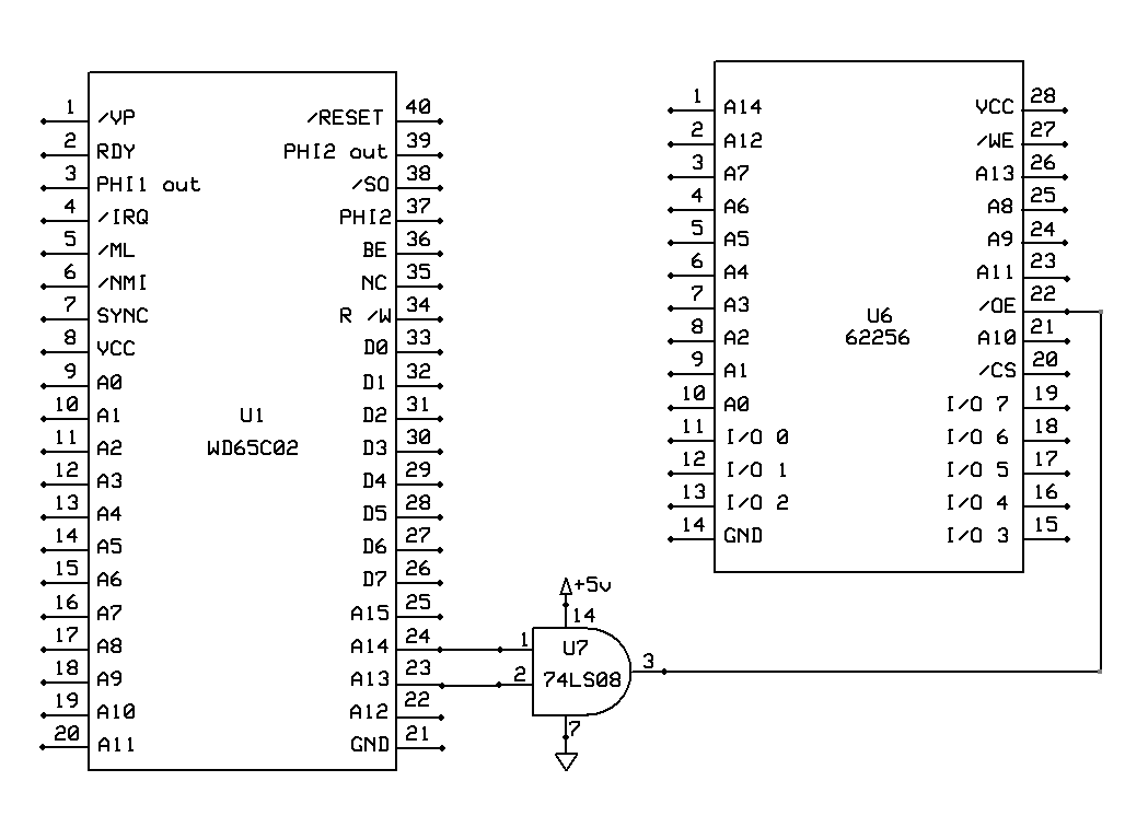
In my documentation for G-Pascal I suggest adding 74LS08 "and" gate to do more fine-tuned address decoding for the RAM, which extends its range to be $0000 to $5FFF.

Ben's description of his project is here.


Top
 Profile  
Reply with quote  
PostPosted: Wed Mar 23, 2022 12:43 am 
Offline
User avatar

Joined: Fri Aug 30, 2002 1:09 am
Posts: 8541
Location: Southern California
Nick Gammon wrote:
Sheep64 wrote:
The best documentation for this design can be found at http://wilsonminesco.com/

I can't see any reference to Ben Eater on that site.

I think what he meant was that Ben seems to have gotten his designs from my site, whether directly or indirectly—although this address decoding scheme is definitely not so absolutely brilliant that no one else could have come up with it. I started using it 30 years ago, published it here 21 years ago in my "Tip of the Day" column at viewtopic.php?p=2326#p2326, and then on my own site 10 years ago.

_________________
http://WilsonMinesCo.com/ lots of 6502 resources
The "second front page" is http://wilsonminesco.com/links.html .
What's an additional VIA among friends, anyhow?


Top
 Profile  
Reply with quote  
PostPosted: Wed Mar 23, 2022 12:45 am 
Offline
User avatar

Joined: Wed Mar 09, 2022 9:08 pm
Posts: 18
Thanks, that clears that up. The address decoding seems straightforward to me. :)


Top
 Profile  
Reply with quote  
PostPosted: Wed Mar 23, 2022 1:42 am 
Offline
User avatar

Joined: Fri Dec 11, 2009 3:50 pm
Posts: 3367
Location: Ontario, Canada
Nick Gammon wrote:
The address decoding seems straightforward to me. :)
Just checking, but did you notice how address line A14 connects to both the A14 input of the RAM and the OE# input of the RAM? :shock: It's not what I would call straightforward. At first I thought Garth had made an error in his schematic!

-- Jeff


Attachments:
basic6502schem.jpg
basic6502schem.jpg [ 465.57 KiB | Viewed 1169 times ]

_________________
In 1988 my 65C02 got six new registers and 44 new full-speed instructions!
https://laughtonelectronics.com/Arcana/ ... mmary.html
Top
 Profile  
Reply with quote  
PostPosted: Wed Mar 23, 2022 2:54 am 
Offline
User avatar

Joined: Wed Mar 09, 2022 9:08 pm
Posts: 18
Ah yes, I leveraged off that to increase the addressable RAM from 16kB to 24kB by "and"ing A14 and A13.

Image


Top
 Profile  
Reply with quote  
PostPosted: Wed Mar 23, 2022 5:36 am 
Offline
User avatar

Joined: Wed Feb 13, 2013 1:38 pm
Posts: 589
Location: Michigan, USA
Hi Nick (and group):

Since you've added a second 'glue' chip to the Wilson (Eater?) design to increase the amount of RAM available, may I suggest a relatively simple and flexible (untested) 2-chip method that even includes a few device select strobes? Of course it does rely on the active high chip select input on a 64K (or 128K) SRAM chip.

Stay safe, guys. Cheerful regards...


Attachments:
temp2.png
temp2.png [ 171.16 KiB | Viewed 1158 times ]


Last edited by Michael on Wed Mar 23, 2022 6:30 pm, edited 2 times in total.
Top
 Profile  
Reply with quote  
PostPosted: Wed Mar 23, 2022 11:05 am 
Offline
User avatar

Joined: Wed Mar 09, 2022 9:08 pm
Posts: 18
GARTHWILSON wrote:
I think what he meant was that Ben seems to have gotten his designs from my site, whether directly or indirectly—although this address decoding scheme is definitely not so absolutely brilliant that no one else could have come up with it. I started using it 30 years ago, published it here 21 years ago in my "Tip of the Day" column at viewtopic.php?p=2326#p2326, and then on my own site 10 years ago.


I believe in giving credit where it is due, so I have amended my main page about G-Pascal to add a link to your site, and also a paragraph suggesting that people look there for more detail about the design.

I also added a link to this forum and the Ben Eater subreddit.


Top
 Profile  
Reply with quote  
PostPosted: Wed Mar 23, 2022 11:06 am 
Offline
User avatar

Joined: Wed Mar 09, 2022 9:08 pm
Posts: 18
Michael wrote:
Since you've added a second 'glue' chip to the Wilson (Eater?) design to increase the amount of RAM available, may I suggest a relatively simple and flexible (untested) 2-chip method that even includes a few device select strobes?


Hi Michael,

Thanks for the suggestion.


Top
 Profile  
Reply with quote  
PostPosted: Wed Mar 23, 2022 6:48 pm 
Offline
User avatar

Joined: Wed Feb 13, 2013 1:38 pm
Posts: 589
Location: Michigan, USA
You're welcome. And thank you for sharing your Pascal project. I'm anxious to try it out.

BTW, you could still use a single chip with coarse address decoding for 32K ROM, 8K I/O, and 24K RAM, but, like the previous example, the example below relies on the extra active high chip select input on a 64K (or 128K) RAM IC.

Cheerful regards, Mike, K8LH


Attachments:
Beater 08c.png
Beater 08c.png [ 527.54 KiB | Viewed 1109 times ]
Top
 Profile  
Reply with quote  
PostPosted: Thu Mar 24, 2022 2:14 am 
Offline

Joined: Fri Dec 21, 2018 1:05 am
Posts: 1114
Location: Albuquerque NM USA
Hi Nick,
I try to port your G-Pascal to my CPLD6502 hardware that emulates Ben Eater's memory map. i.e., Flash from $8000-$FFFF, RAM from $0-$5FFF, and W65C22 from $6000-$7FFF. My original CPLD6502 has no W65C22 so I built a prototype board that plugs into CPLD6502's expansion bus. CPLD6502 is proven hardware I'm comfortable with but the W65C22 prototype is new.

I download your design from GitHub earlier this week. I burn a flash with the binary file, gpascal.bin. I made sure the program resided in $8000-$FFFF. Powering up I was expecting some activities on the serial port which is wired to PA0 and PA1 (PA0 is also connected to CB2 for falling edge interrupt), but I didn't see any activities while monitoring with a scope. When I send a character to the serial port, I can see interrupt generated to W65C02 but the interrupt stayed low, apparently it was never serviced.

I do not have 2-line LCD display but do have a 4-line LCD display. I hook up the 4-line LCD display (PA5 to RS, PA6 to RW, PA7 to E, PB0 to D0, PB1 to D1, PB2 to D2, etc to PB7 to D7), but it also showed no activities while monitoring RS, RW, E with scope.

I looked into gpascal.list listing and traced the execution of power-on reset, observed "hardware_init" routine being executed where VIA_PORTA, VIA_DDRA, VIA_ACR, VIA_PCR, VIA_T1C_L, VIA_T1C_H, VIA_IER, VIA_IFR are initialized with the right values. Yet VIA did not seem to be working.

Suspecting VIA prototype is the problem, I wrote a couple simple programs to exercise PA0, PA1, Timer1, interrupt, VIA_IER, VIA_IFR. They all worked as expected. I'm kinda stuck right now.

Is the software waiting on some inputs after power applied before output the sign-on message on serial port and/or LCD display? Is there a heart beat signal I can monitor such as interrupt? Is LCD display constantly being updated so I should see activities on LCD's RS/RW/E lines? Are there monitor/diagnostic embedded in gpascal.bin that I can patch into? Thanks for your help.
Bill


Top
 Profile  
Reply with quote  
PostPosted: Thu Mar 24, 2022 4:14 am 
Offline
User avatar

Joined: Wed Mar 09, 2022 9:08 pm
Posts: 18
Try re-assembling with:

Code:
LCD_SUPPORT = 0


in gpascal.asm.

That way it should basically not do much with the 6522 VIA. I thought I had a time-out in the LCD code if it didn't initialise quickly enough but perhaps not. If that turns out to be the issue I'll have a closer look at that code.

The other thing is, does it emulate the WDC65C02 instructions? I used some of the newer ones like TSB and TRB. If they are not implemented the CPU may hang or generate interrupts.

Quote:
Is there a heart beat signal I can monitor such as interrupt?


There is an interrupt on T1 at the baud rate (4800/sec if you are using a 1 Mhz clock) however that is not active unless it is actively sending bytes. It does in fact send bytes at the start (the welcome message) so there should be activity in the IRQ routine shortly after startup ... unless it got hung up doing the LCD stuff.

The only way I can realistically generate heartbeat pulses is using the VIA, and the VIA is the thing in doubt right now. :)


Top
 Profile  
Reply with quote  
PostPosted: Thu Mar 24, 2022 2:24 pm 
Offline

Joined: Fri Dec 21, 2018 1:05 am
Posts: 1114
Location: Albuquerque NM USA
A night's rest and assurance from the designer that I'm on the right track is the best troubleshooting technique. Because I don't need 512K RAM in this situation, I used a smaller 128K RAM (AS6C1008) instead. I forgot Address 17 (pin 30) in 128K RAM is chip select and need to be driven high otherwise the program will crash upon first return from subroutine. Boy, it sure did.

Once 128K RAM's active-high chip select is driven high, the original program booted just fine. The clock is 12MHz so serial port is running at 57600. The 4-line LCD display worked even at 12MHz; I noticed it needs local echoback and use line feed instead of carriage return. Thank you for your help.

Bill


Attachments:
DSC_69170324.jpg
DSC_69170324.jpg [ 1.44 MiB | Viewed 1057 times ]
Top
 Profile  
Reply with quote  
Display posts from previous:  Sort by  
Post new topic Reply to topic  [ 71 posts ]  Go to page Previous  1, 2, 3, 4, 5  Next

All times are UTC


Who is online

Users browsing this forum: No registered users and 1 guest


You cannot post new topics in this forum
You cannot reply to topics in this forum
You cannot edit your posts in this forum
You cannot delete your posts in this forum
You cannot post attachments in this forum

Search for:
Jump to: