6502.org Forum  Projects  Code  Documents  Tools  Forum
It is currently Sat Oct 05, 2024 5:39 pm

All times are UTC


Post new topic Reply to topic  [ 33 posts ]  Go to page Previous  1, 2, 3
Author Message
PostPosted: Thu Dec 23, 2021 7:03 pm 
Offline
User avatar

Joined: Mon Aug 30, 2021 11:52 am
Posts: 287
Location: South Africa
[Edit - My previous reply is on page 2]

Right, I've tried with a 5MHz clock oscillator.

As before the clock signal is yellow, the green is ÷ 2 and triggers at 2.50000MHz. The cyan is ÷ 4 and triggers at 1.25000MHz

The pink is still the 3.3V line and I'm not sure what to make of it.

Attachment:
SDS00009.png
SDS00009.png [ 32.41 KiB | Viewed 262 times ]


I check what sort of difference the probe placement would make and their definitely is a difference. The cyan (front) signal is the probe attached to the 0.65mm traces on the IC (that was fun :| ) and the yellow (behind) is the probe attached to the pins and wire. Swapping the probes around produces the opposite result (yellow falls exactly where cyan does in the picture) so it's consistent.

Attachment:
SDS00008.png
SDS00008.png [ 24.59 KiB | Viewed 262 times ]


ps: Turns out the 25MHz clock oscillator I have is a 5mm by 3.2 package and that was just going to be too much of a mission to solder in.


Top
 Profile  
Reply with quote  
PostPosted: Wed Dec 29, 2021 4:31 pm 
Offline
User avatar

Joined: Mon Aug 30, 2021 11:52 am
Posts: 287
Location: South Africa
I've been having a bit of an experiment :D

I've managed to go from this awful signal here:
Attachment:
20211228_201827.jpg
20211228_201827.jpg [ 88.26 KiB | Viewed 214 times ]


to this:
Attachment:
Timing.png
Timing.png [ 42.24 KiB | Viewed 214 times ]


I'm quite chuffed with the result although I still not sure what I'm doing. Basically throwing components at it until I ... invented the RC filter? I dunno.

I'm getting quite good with the scope too, or at least judging when I'm getting a real signal vs when it's struggling. I broke out my aging 50Mhz Tektronix for comparision. The poor thing has never been used for anything outside of the KHz range but it slogged along well at 50MHz. I can also confirm that whilst not garbage, the probes that came with the Siglent are not great; I'm definitely going to have to invest in something better.

In the graph the white line rises from 0.4V to 2.0V. I was curious how long I was in the valid ranges in 3.3V LVC. I don't know why I measured from 0.4, the low level should be 0.8 which makes everything EVEN BETTERER!

Attachment:
Buffered Timer.jpg
Buffered Timer.jpg [ 111.28 KiB | Viewed 214 times ]

Quite a lot of the solution was pulling all the signal pins out of the stripboard and soldering them directly together. The resistors are there to stop the ringing, I haven't seen anyone else do this but it works. Comments on what I should be doing would be most appreciated 8)

The Frankensteined caps on the 74LVC74 flip-flop was left over experimentation; I could probably have used a single 1.0nF or 0.1nF bypass capacitor. The clock oscillator is 100Mhz HCMOS whose output is fed into the flip-flop as a clock divider and from there it's two outputs (Q and /Q) are fed into the two 74LCV1G34 buffers.

I should mention I'm getting about 0.5V peak-to-peak noise on my 3.3V line (mostly around the flip-flip) I think the only real way to solve that is to go to a PCB.

The short of it is: even if there is a better way to get the 50MHz and inverse signal I need (and I hope there is) now I know I can do this. That gives me hope for building the rest of the timing signals I need!


Top
 Profile  
Reply with quote  
PostPosted: Wed Dec 29, 2021 7:47 pm 
Offline
User avatar

Joined: Fri Dec 11, 2009 3:50 pm
Posts: 3367
Location: Ontario, Canada
Quote:
I'm getting about 0.5V peak-to-peak noise on my 3.3V line
For those not yet well versed in the use of oscilloscopes, it's a highly worthwhile exercise to spend some time scoping the ground connections of your project. You might expect ground to read as just a flat line, but that's rarely what you'll see when there's fast logic that's switching nearby.

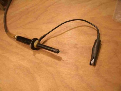
As you improve your technique (and this depends heavily on the use of a short ground lead on your scope probe, as shown in the photo) you'll see ground get quieter and quieter on the screen. Probably you won't achieve the ideal, perfectly flat line, but do give it some effort before you decide it's "good enough."

The point is, the scope will usually be showing you a certain amount noise that's not relevant, such as the noise picked up by a probe ground lead that's excessively long, attached to the wrong point in the project, or -- worst of all! -- simply absent. Your first line of defense is to limit stray noise pickup as much as you reasonably can. Then step two is to apply a mental fudge factor.

So, for example, if you scope the ground pin of an IC then scope the Vcc pin, and both pins seem to have the same type and amount of noise, then no problem is indicated WRT the power to that IC -- even though you may seem to have "about 0.5V peak-to-peak noise" on the Vcc pin.

-- Jeff

PS- Andrew, I'm not suggesting your observation is wrong, just saying that all such observations have potential to be misleading. Also, even the "short" ground lead in the photo is longer than ideal -- a compromise.

Image

_________________
In 1988 my 65C02 got six new registers and 44 new full-speed instructions!
https://laughtonelectronics.com/Arcana/ ... mmary.html


Top
 Profile  
Reply with quote  
Display posts from previous:  Sort by  
Post new topic Reply to topic  [ 33 posts ]  Go to page Previous  1, 2, 3

All times are UTC


Who is online

Users browsing this forum: No registered users and 29 guests


You cannot post new topics in this forum
You cannot reply to topics in this forum
You cannot edit your posts in this forum
You cannot delete your posts in this forum
You cannot post attachments in this forum

Search for:
Jump to: