Ultimately, I would love nothing more than to have my own PCB manufactured, but I have no idea, no ability and no confidence on being able to do that at the moment. Any pointers on this aspect would be gratefully received.
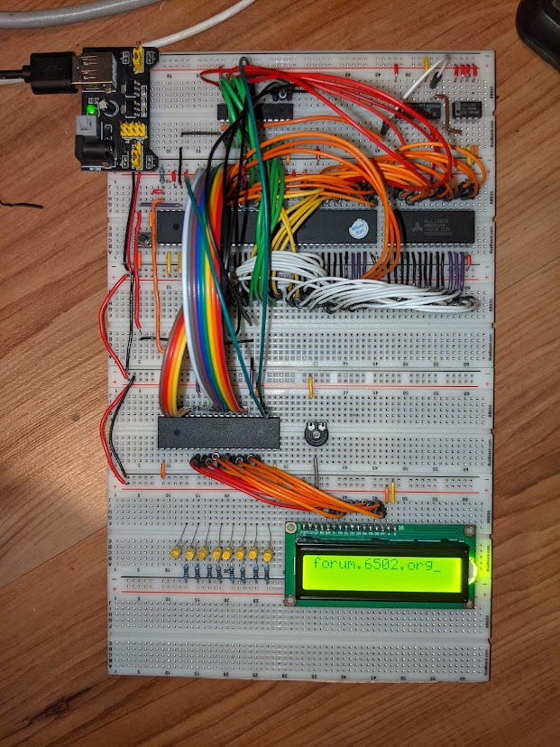
Great story, great job, and indeed well done on that breadboard! That is definitely an accomplishment!
I know I am definitely the newbie here, but I saw Gordon's comment and felt I needed to chime in some. I use KiCad exclusively now (on Linux), and it does have a learning curve, but not as steep as I would have first imagined. I had been using some other junky program before that. I didn't even realize how junky it was until I switched to KiCad.
Some things I have learned about KiCad (and anyone else, tell me if you think I'm wrong):
1) It wants you to do a schematic first, THEN the PCB. KiCad is all about it's netlist, and if you are not following it, it will flag errors when you debug the board on the software. For a long while I just ignored all that, and did my own thing. But when I was recently designing my first board that I was actually going to have printed, I said "eh, I got time, lets try this netlist thing out". Good thing I did, I flipped some wires! [ I seem to do that a lot... ]
2) Using 2-layers on KiCad is super easy, but the 4-layer stuff is weird. I basically had to make 2 additional layers, tell it to make a copper pour on those layers, and then manually change any pins or vias netname, one by one by one by one. This cool plugin for KiCad called "WireIt" really helped a LOT when doing this netlist stuff, especially with the 4-layers.
3) Maybe it's just my version, but the thing bugs out a lot. Like when I switch between layers, the program says I'm on the top layer AND the bottom layer, so you just gotta 'know' what's going on. Likewise, sometimes when I put a new footprint on the board, the whole thing goes wild and flashy until I restart it. Again, that just might be mine.
4) As far as what size traces, spaces, vias, etc, that I had to discover over time. With Garth and BDD's help (and previous posts on the forum) I found some sizes that worked for me:
0.2 mm signal traces and spaces
1.6 mm power traces
0.9 / 0.4 mm vias for signals
I set my grid at 25 mils, and I can get signal lines in between the DIP footprint pins which is VERY important.
5) Start simple. Don't go full netlist stuff on the first try, because it'll just be frustrating. Don't do a schematic that will transport directly over to PCB-land, you'll just have this huge rats nest that would be confusing. Just start up pbcnew (that's it's particular name on the KiCad suite) and playing around with it. Start with the Edge.Cuts layer, make/draw a rectangle. Then add a DIP package footprint. Then use the default trace/via sizes and just connect things on F.Cu and B.Cu layers. Just play around with it before getting serious. Use their built in 3D viewer to have that sense of accomplishment every couple of hours. Be ok with ditching what you have been working with and starting new. I do that often, when my traces around the glue logic look ugly or something, I just delete it all and start over again. Before I sent off for my printed 4-layer board, I went through 10+ different KiCad board designs.
What I do not suggest (unless you like to learn a lot) is to buy perf board and solder each wire by-hand. That's what I did, and well, it worked eventually with some great help from folks here on the forum. But that was unnecessarily crazy. If you have $20 to spend on a printed board, print the board and save your time and energy (and even money).
Lastly Gordon suggested JLCPCB, and I definitely recommend them as well. Super cheap 10cm x 10cm boards, so if you keep it small and tight (seems impossible at first, but totally doable with what you have it seems) the cost is significantly less. I ended up printing two separate 10x10 boards which I will solder together to make a 10x20 board basically. WAY cheaper than having a single 10x20 board printed.
Anyone else, feel free to disagree with me, I am still the newbie here. I just really like KiCad and had to leave a comment. Thanks!
Chad
EDIT: One last thing, JLCPCB has a super awesome tutorial on how to grab the gerber/drill files from KiCad. It was such a good tutorial I bookmarked it.
https://support.jlcpcb.com/article/149- ... s-in-kicad