6502.org Forum  Projects  Code  Documents  Tools  Forum
It is currently Fri Nov 22, 2024 10:10 am

All times are UTC


Post new topic Reply to topic  [ 56 posts ]  Go to page 1, 2, 3, 4  Next
Author Message
 Post subject: 65816 Logisim Project
PostPosted: Wed Oct 13, 2021 6:56 pm 
Offline
User avatar

Joined: Mon Aug 30, 2021 11:52 am
Posts: 287
Location: South Africa
Hi all! First post here and it's because I need a bit of help.

Is anyone familiar with writing Logisim libraries? I've written a (half) cycle accurate 65c816 emulator that I had intended to drop into Logisim but I do not understand how Logisim's port propagation works.

If you take a look at the image below you'll see that the value on the bus port D is 'C9' but the value I read off that port is zero. 'C9' does eventually appear on the port but only after I'm long done ticking the CPU.

Image

I'm guessing it's because it takes a while for the simulation to settle between each clock tick but I'm at a loss as to how to handle it.

Any help would be great! Ta, Andrew


Attachments:
Logisim65816.png
Logisim65816.png [ 19.45 KiB | Viewed 16743 times ]
Top
 Profile  
Reply with quote  
PostPosted: Thu Oct 14, 2021 11:12 am 
Offline
User avatar

Joined: Thu Dec 11, 2008 1:28 pm
Posts: 10985
Location: England
Welcome, Andrew, sorry to say I can't help. Is there a waveform view or similar which will show the time-varying behaviour of the bus?

As the databus is bidirectional it may need special handling of some kind: event driven simulators don't always have a graceful way to handle data propagation in both directions.


Top
 Profile  
Reply with quote  
PostPosted: Thu Oct 14, 2021 7:23 pm 
Offline
User avatar

Joined: Mon Aug 30, 2021 11:52 am
Posts: 287
Location: South Africa
Hey BigEd, thanks for the welcome. I was putting together a (kind of) time based view thing when I got distracted by something I broke. I'll post it either tomorrow or the weekend depending on how long it takes clean it up and make it human readable.

I'm pretty sure you're right that it's got something to do with bidirectional data (and how that complicates how long it takes for the simulation to settle).


Top
 Profile  
Reply with quote  
PostPosted: Thu Oct 14, 2021 7:30 pm 
Offline
User avatar

Joined: Thu Dec 11, 2008 1:28 pm
Posts: 10985
Location: England
I don't know how Logisim does its thing, but some simulators will distinguish minor iterations that are needed to get values to settle from major iterations which move time forward. So, time would not elapse even if it takes some work to figure out the next state.

Does Logisim model propagation delays at all?


Top
 Profile  
Reply with quote  
PostPosted: Fri Oct 15, 2021 6:51 pm 
Offline
User avatar

Joined: Mon Aug 30, 2021 11:52 am
Posts: 287
Location: South Africa
Logisim does model propagation delays but only in certain limited circumstances - circumstances I can't find any real documentation on.

However all of that said I think it's a much simpler program bug on my part. I've been using Solra Bizna's 6502 Logisim emulator as an example and, reduced to the simplest possible state of just reading the data bus, his works and mine does not. Even though they look pretty much identical to me. I'm just going keep slogging looking for the difference. It could be worse, I could not have a working example to compare mine to :?

Just for interests sake I've fixed up the circuit a bit and included the (working) 65C02 so I run the two side by side.


Last edited by AndrewP on Mon Oct 18, 2021 5:25 pm, edited 1 time in total.

Top
 Profile  
Reply with quote  
PostPosted: Mon Oct 18, 2021 5:25 pm 
Offline
User avatar

Joined: Mon Aug 30, 2021 11:52 am
Posts: 287
Location: South Africa
It finally works!

In the end it turned out it was 'just' a Logisim propagation issue. The short of it is that doing a read from memory takes a few steps to settle before the propagation cycle ends. However I only want the CPU to truly tick on the very last cycle once everything has settled. A bit of a problem as Logisim doesn't seem to have hooks for notifying me when a propagation cycle is starting or for when it's done.

Still a small hack and I can tell I've transitioned from a stable state to a new propagation cycle. Built on that is a slightly larger (but pretty robust) hack that only moves the CPU into its new stable state at the start of the next propagation cycle rather than at the end of its actual propagation cycle.

Long story short: WHY DID WDC MULTIPLEX OUT THE BANK ADDRESS ON THE DATA PINS, why not re-use the address pins instead? Gaaaaaa! Writing out the BA on the data pins a half-cycle before a read on those same pins caused Logisim no end of grief. But in the end any complex circuit with half-cycle reads/writes would have been a problem - regardless of the pins multiplexed. It's probably better I discovered that sooner rather than later.
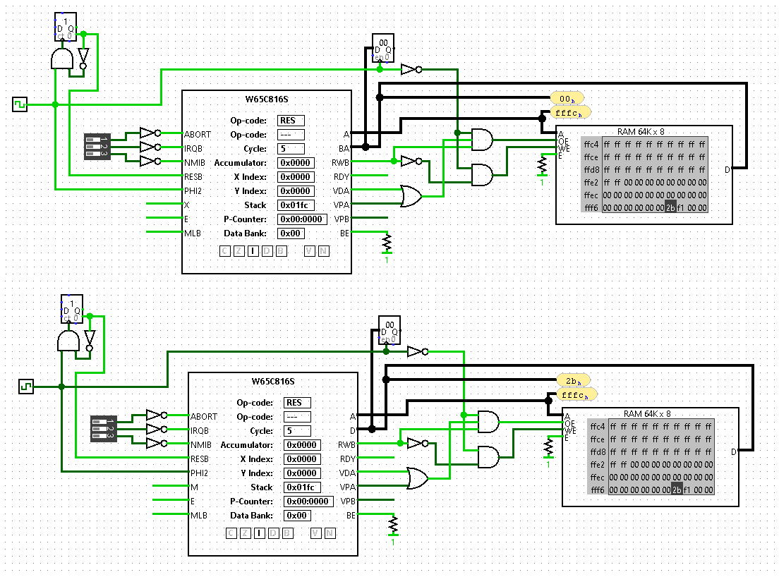
Image

Above you can see a simple circuit that correctly latches in the Bank Address (zero in this case) when the clock is high and also correctly reads 2b out of memory when the clock is low. It happens to be pulling the low byte of the RESET vector in the picture. That was quite an adventure :shock:

A bit later I'll post up some of the timings from the little program I'm running as I'm quite chuffed with it. Right now, it's supper time


Top
 Profile  
Reply with quote  
PostPosted: Mon Oct 18, 2021 5:47 pm 
Offline
User avatar

Joined: Fri Aug 30, 2002 1:09 am
Posts: 8543
Location: Southern California
AndrewP wrote:
Long story short: WHY DID WDC MULTIPLEX OUT THE BANK ADDRESS ON THE DATA PINS, why not re-use the address pins instead?

The way they did it makes all 24 address bits valid at once, well ahead of the rise of phase 2, for an early start at address decoding, as required by many of the 65xx I/O ICs which must have their chip selects, register selects, and R/W signals all valid well ahead of the rise of phase 2. What I wish they had done is just go to a 48-pin DIP (or better, a PLCC), with no multiplexing.

_________________
http://WilsonMinesCo.com/ lots of 6502 resources
The "second front page" is http://wilsonminesco.com/links.html .
What's an additional VIA among friends, anyhow?


Top
 Profile  
Reply with quote  
PostPosted: Mon Oct 18, 2021 6:03 pm 
Offline
User avatar

Joined: Mon Aug 30, 2021 11:52 am
Posts: 287
Location: South Africa
GARTHWILSON wrote:
The way they did it makes all 24 address bits valid at once, well ahead of the rise of phase 2
Ah. Yes. That's a good point. Oops.
I'd also dearly love a non-multiplexed version; I guess that's a common comment.


Top
 Profile  
Reply with quote  
PostPosted: Mon Oct 25, 2021 3:04 pm 
Offline
User avatar

Joined: Mon Aug 30, 2021 11:52 am
Posts: 287
Location: South Africa
I finally solved the hacks I mentioned previously. I needed to make a tiny change to Logisim to get the event hooks I wanted (a literal 4 line change). I've submitted a pull request for that change so hopefully it will be included in the next release.

For now, at least in terms of emulating the WDC65C816, I'm declaring it "good enough". The emulation works with the simple program I need to test address decode circuitry* and interrupt vectors.

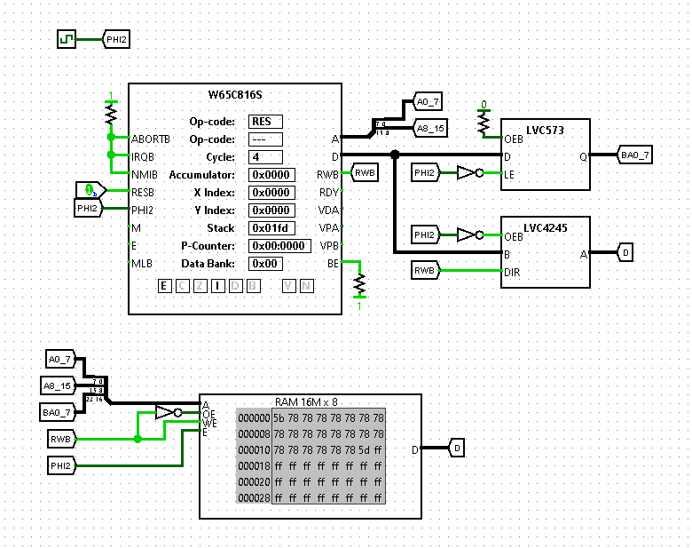
Image

I'm now pretty good at banging out Logisim components so I've added the standard latch and transceiver suggested in the datasheet as a kind of proof of concept. Eventually I'm going to code up all the ICs I think I'll need.

If anyone REALLY wants these components now drop me a message and I'll point you to them but I've still got a lot of cleanup to do before I want to do a public release.

*If anyone has a functional test suite of 65816 opcodes that would be great though.


Top
 Profile  
Reply with quote  
PostPosted: Mon Oct 25, 2021 5:01 pm 
Offline
User avatar

Joined: Thu Dec 11, 2008 1:28 pm
Posts: 10985
Location: England
> If anyone has a functional test suite of 65816 opcodes that would be great though.

Dave/hoglet reminds us of Drass' current efforts towards an '816 test suite:
viewtopic.php?p=87939#p87939


Top
 Profile  
Reply with quote  
PostPosted: Mon Oct 25, 2021 8:48 pm 
Offline
User avatar

Joined: Thu May 28, 2009 9:46 pm
Posts: 8505
Location: Midwestern USA
AndrewP wrote:
Long story short: WHY DID WDC MULTIPLEX OUT THE BANK ADDRESS ON THE DATA PINS, why not re-use the address pins instead?

As Garth said, it is so the entire 24-bit address is presented at the same time and during Ø2 low. Sequentially emitting the address in two parts would result in a timing nightmare of the worst kind.

The historical reason for multiplexing A16-A23 has to do with Apple's desire to stay with the PDIP-40 package. In those days, SMT package forms, such as PLCC and TSOP, were barely in their infancy and there was some resistance to moving away from the DIP format that had long been in use. With 40 pins on the PDIP package, there wasn't any way to make A16-A23 appear as separate outputs. Hence the MUXing.

As Garth noted, it would be nice if the MUXing "feature" were eliminated by offering the 816 in a bigger package. The next size up in PLCC would be PLCC52, which would offer enough pins to bring out A16-A23 on separate connections. It could also be done in PDIP48, although that would make for a bulky package that might also have some subtle electrical issues with ground bounce (the PLCC package has multiple ground pins).

_________________
x86?  We ain't got no x86.  We don't NEED no stinking x86!


Top
 Profile  
Reply with quote  
PostPosted: Tue Oct 26, 2021 1:22 pm 
Offline
User avatar

Joined: Mon Aug 30, 2021 11:52 am
Posts: 287
Location: South Africa
BigEd wrote:
Dave/hoglet reminds us of Drass' current efforts towards an '816 test suite:
viewtopic.php?p=87939#p87939
That's excellent! Thanks for pointing me there (and I should probably go drop a message in Drass' original thread)

BigDumbDinosaur wrote:
Sequentially emitting the address in two parts would result in a timing nightmare of the worst kind.
Yup, I was tired and having a frustrated-with-Logisim-brain-shutdown moment. I really wish the 65C256 was less microcontroller'y and more a 65C816 with 24 address pins and a bunch of separately vectored priority IRQs. That would be perfect for me :D


Top
 Profile  
Reply with quote  
PostPosted: Thu Oct 28, 2021 12:29 pm 
Offline
User avatar

Joined: Mon Aug 30, 2021 11:52 am
Posts: 287
Location: South Africa
Tiny update I'm using mostly as an excuse to post more pictures.

The pull request I submitted was rejected which I kind of both can and can't be a bit miffed about. I didn't follow their coding guidelines even though I'd followed an existing pattern. That shouldn't have been a problem; I just had to rename the bad method and commit. Except I'd done a bunch of other experimenting in the branch I'd submitted and that would have all gone too. In the end I got into such a tangle of branches trying to get only the commits I wanted that I had to delete and re-fork the whole project. Gah.

On the brighter side I may have found a better work around if my new pull request is also rejected. It's not pretty but seems to be the existing pattern (again) for determining if the simulation has completed a tick.

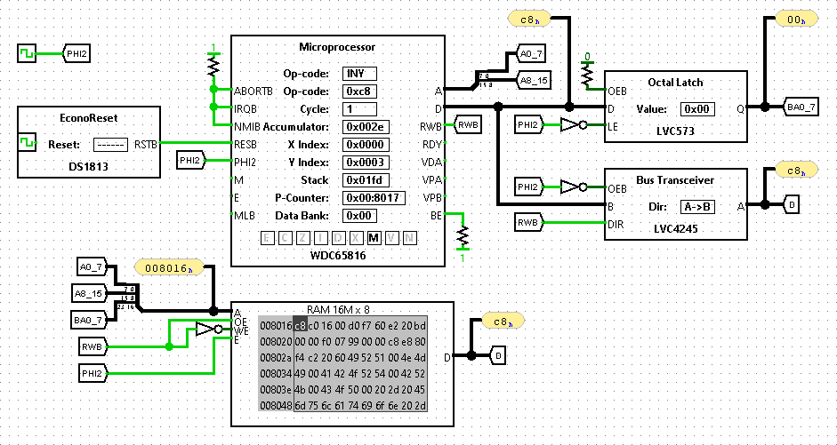
Image

The EconoReset was a bastard to write. A component without a connected clock does not tick but the EconoReset should be it's own clock and tick internally for however long the reset line needs to be held low. In the end I finally just embedded a clock in the thing and gave up.


Top
 Profile  
Reply with quote  
PostPosted: Fri Nov 05, 2021 6:31 pm 
Offline

Joined: Sat Apr 11, 2020 7:28 pm
Posts: 344
I only post here to remember all of you that the w65c265 is a MCU offered in 84 pin PLCC or 100 pin QFP packages, that features a full exposed 24 bit address bus with no need of demultiplexing at all.

AFAIK you can use it as a regular '816 if you program it to behave as such during boot by the use of an external ROM.

It features an internal chip select mechanism but if you decide to use it as a '816, then you should manage the chip selects externally as you would do with an standard '816.

People with more experience that me (easy to find) will tell about logic or coding differences between an '816 and the '816 core inside the '265.

I asked WDC about the MCU and they said that right as it's being sold, is just a development platform, not focused to hobbyists or consumers but developers that would use it to refine and debug a code up to the point of being definitive or RELEASE, and then ask WDC for a quote of a custom design where the internal monitor ROM would be replaced by the custom ROM, and then, things like 576 bytes of RAM would make sense in the MCU workd.


Top
 Profile  
Reply with quote  
PostPosted: Sun Dec 12, 2021 3:53 pm 
Offline
User avatar

Joined: Mon Aug 30, 2021 11:52 am
Posts: 287
Location: South Africa
tokafondo wrote:
I only post here to remember all of you that the w65c265 is a MCU offered in 84 pin PLCC or 100 pin QFP packages, that features a full exposed 24 bit address bus with no need of demultiplexing at all.

Thanks, I saw it and took a look at it some time ago. And (if memory serves) it had two problems for what I want to do. It is too expensive (I'm going to ultimately be using five 65816s if I can actually make things work and that's a significant cost). And two it's top speed is officially 8MHz; I'm going to need to use an asymmetric duty cycle with the low part of the cycle running at an effective 25Mhz. I'm pretty certain the W65C816S6TQG-14 will be able to handle it but I'm not certain about W65C265.


Top
 Profile  
Reply with quote  
Display posts from previous:  Sort by  
Post new topic Reply to topic  [ 56 posts ]  Go to page 1, 2, 3, 4  Next

All times are UTC


Who is online

Users browsing this forum: No registered users and 7 guests


You cannot post new topics in this forum
You cannot reply to topics in this forum
You cannot edit your posts in this forum
You cannot delete your posts in this forum
You cannot post attachments in this forum

Search for:
Jump to: