6502.org Forum  Projects  Code  Documents  Tools  Forum
It is currently Mon Oct 07, 2024 5:20 am

All times are UTC


Post new topic Reply to topic  [ 62 posts ]  Go to page Previous  1, 2, 3, 4, 5  Next
Author Message
PostPosted: Thu Aug 19, 2021 6:58 pm 
Offline

Joined: Tue Jul 05, 2005 7:08 pm
Posts: 1041
Location: near Heidelberg, Germany
cjs wrote:
Quote:
The /SEL line "outsources" part if the detection process to the main board.

If all you're looking for is to let some boards that do decoding put their decoded selects out on to the bus, read though the previous posts in this dicussion: that's exactly what we plan to do. In fact, some people are already doing this; we just intend to formalize it a bit more. So no fear there.


Yes that's about it. A line that puts a decoded address space on the bus, and that is used by e.g. I/O boards is it.
For example if a /SEL line that decodes a 2k or 4k I/O space, and I/O boards use it, they need just a single '688 to decode 16 bytes of I/O address space, to not collide with other I/O boards.

Similar to what I did here 
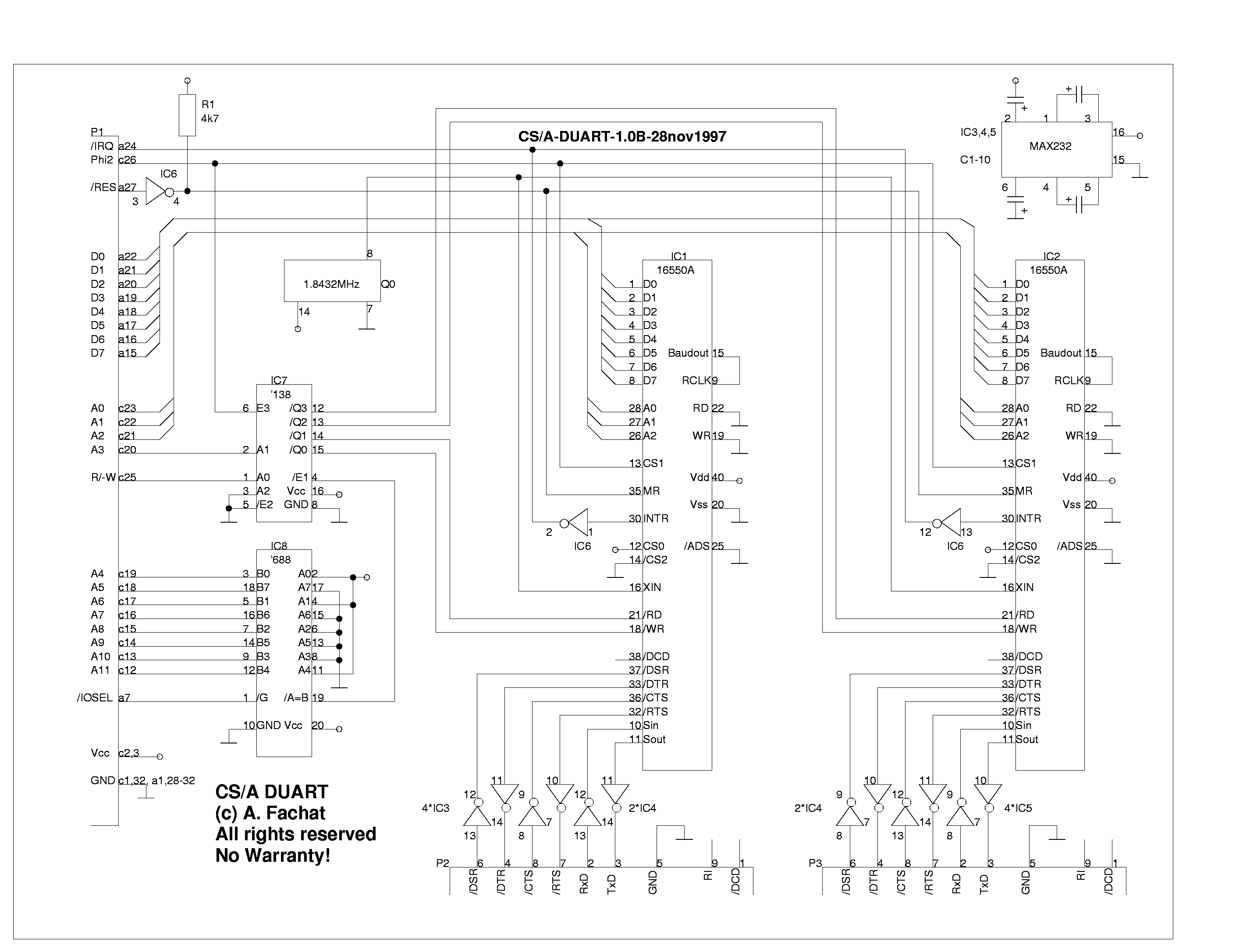
http://www.6502.org/users/andre/csa/bus-1.1.html

Quote:
But you seem to keep bringing (perhaps unwittingly) timing into this discussion. Pardon me if I'm misintepreting you and you're not, but if you are, keep in mind that the address mapping selects will NOT be usable for any timing purposes, just as the address bus itself is not. You'll need to use Φ2 for anything related to timing, just as usual.


I think this is a misunderstanding. 6502 busses use Phi2, no way around it.

Quote:
fachat wrote:
But how is a chip selected? It detects the right value on the address lines.

Right, but that's nothing to do with timing and cannot be used for any sort of timing. The 6502 has full control of the address bus at all times (unless you put a tri-state buffer in front of it to let you cut it off), and you must never assume that the timing of any signal change on the address bus means anything. The same goes for other non-clock lines, too, which is why all writes should always be qualified with Φ2.

Quote:
The z80 sytems IIRC have separate /rd and /wr lines on the bus. Those incorporate the equivalentof the r/-w and phi2 lines of the 6502 - but they can also be qualified with address selection. Not sure it does on RC2014 though.

Yes, as you point out, /RD and /WR are different because they include timing information, unlike RWB or the address bus from either CPU. (Perhaps this is why you sound to me like you're talking about timing.) And being separate signals they also incorporate "enable" communication (unlike RWB) and so could be manipulated by the CPU board not to assert on the bus while at the same time asserting for local peripherals on the CPU board (based on address or anything else). But I don't see anything like that appearing in RC6502 bus or variants of it, that's just too alien to how the Motorola-style buses work. If you wanted to do something like that, it would probably make more sense to put your 6502 on RC2014 bus.


I think we need to look at different types of boards to see the different requirements for an interface
  • A CPU board typically provides timing, direction of data transfer, and address lines
  • An I/O board uses the timing, direction, and address lines to do the transfer

A "select" line is a kind of "abbreviation", in that it selects a limited range of addresses, using the address lines.

Now, let's look at different types of busses, and how they implement the four qualities timing, direction, address, and selection. In the following table I've added my CS/A bus (linked above) to give an impression of what I also imagine for RC6502:
Code:
Bus:        RC6502      CS/A        Z80/RC2014
----------------------------------------------
Timing:     Phi2        Phi2        /RD+/WR
Direction:  r/w         r/w         /RD+/WR
Address     A0-15       A0-11/19    A0-15
Select:      -          /IOSEL      -


The RC2014 bus has only /RD and /WR. They transport timing and direction. Address lines provide addresses. There is no select line, so every board has to provide an own selection circuit using all 16 address bits. However, if just using an I/O board, the selection could be merged into the /RD and /WR lines easily, by ORing /RD and /WR with a /SEL line.

The CS/A bus has the 6502-specific clock Phi2, the r/-w line to tell the direction, and a select line /IOSEL. Here, an I/O board only needs to check the lower 11 address lines, which makes for a simpler circuit. Also, the I/O boards can be mapped to different addresses depending on whether the CPU board (or any other board that is defined to provide it) decodes the /IOSEL line. I used this for example to provide different "personalities" for the machines using this bus, e.g. a 4032 PET that has I/O on $e800-$efff, and a VC1581 disk drive that has I/O in other areas.

The RC6502 as I see it so far, only has Phi2, r/-w, and address lines. An I/O board needs to decode all 16 address lines to select e.g. a single register. That requires are larger detection circuit. However, an I/O board for RC6502 without an /IOSEL can not have I/O mapped to other addresses easily, and it cannot be folded into the Phi2 or r/-w lines. Well, you could probably fold it into phi2 (phi2 -> phi2 and IOSEL), but that may wreak havoc on e.g. a VIA timer.

Quote:
Quote:
But even in a 6502 system like RC6502 this /sel line could mask the bogus read (+writes on the NMOS part) of the 6502, that you'd otherwise have to deal with.

Yeah, it could, but then you put a huge implementation burden on everybody making boards that drive that line to implement the timing for it correctly, and all old RC6502 CPU boards need non-trivial modifications to do this, if it can be done at all. If you're going to go that route, I'd say you're making a new bus.


/sel does not need to have timing quality (in the meaning as above) - it's just decoded address lines. You could just have a "personality" board that has some ROM, and decodes an I/O window in that ROM to be used for I/O and selects /IOSEL in that area. And then provide different "personality" boards for the different systems you want to "emulate". Or use a jumper on the ROM board (or ROM/RAM board).

I don't think we're even far apart in the end. I'm just arguing for an /IOSEL line that I/O boards should incorporate into their address decoding logic. Because, IMHO it's just only advantages (except the one bus line used).

André

_________________
Author of the GeckOS multitasking operating system, the usb65 stack, designer of the Micro-PET and many more 6502 content: http://6502.org/users/andre/


Top
 Profile  
Reply with quote  
PostPosted: Thu Aug 19, 2021 7:16 pm 
Offline

Joined: Tue Jul 05, 2005 7:08 pm
Posts: 1041
Location: near Heidelberg, Germany
Here is just a simple example of a dual-UART board I made for a bus that has an /IOSEL line:

http://www.6502.org/users/andre/csa/duart/csaduart.png

It's just using a single '688 to select a 16 byte I/O window out of the 2k/4k (jumper on CPU) I/O window for /IOSEL. And then it uses a simple '138 to combine Phi2, R/-W, A3 and the /SEL for that 16 byte window to create the /RD and /WR lines for the two UARTs.

The point I'm trying to make is that such an /IOSEL line a) reduces the required address decoding logic on many I/O boards, and b) allows the use of the same I/O board in different types of systems that want to map the I/O area into different places in the address space (by moving the /IOSEL area around).

_________________
Author of the GeckOS multitasking operating system, the usb65 stack, designer of the Micro-PET and many more 6502 content: http://6502.org/users/andre/


Top
 Profile  
Reply with quote  
PostPosted: Thu Aug 19, 2021 7:59 pm 
Offline
User avatar

Joined: Thu May 28, 2009 9:46 pm
Posts: 8416
Location: Midwestern USA
fachat wrote:
The point I'm trying to make is that such an /IOSEL line a) reduces the required address decoding logic on many I/O boards, and b) allows the use of the same I/O board in different types of systems that want to map the I/O area into different places in the address space (by moving the /IOSEL area around).

Even Commodore was aware of the benefit of already-decoded selects at the cartridge port. In particular, there were /IO1 and /IO2, which appeared at $DExx and $DFxx, respectively. The only nuisance thing with those signals is they weren't asserted until Ø2 high.

A similar principle, although much more sophisticated, is used with PC-style expansion buses.

As an aside, it has often been recommended to not take the MPU's buses off-board. Aside from loading issues due to parasitic capacitance, transmission line effects can arise and sabotage performance.

_________________
x86?  We ain't got no x86.  We don't NEED no stinking x86!


Top
 Profile  
Reply with quote  
PostPosted: Thu Aug 19, 2021 11:42 pm 
Offline
User avatar

Joined: Fri Jun 25, 2021 5:38 am
Posts: 72
Location: Portland, Oregon, USA
I think we all agree on /IOSEL providing benefit. So... /IOSEL on pin 39 (formerly known as EX2) or on pin 26 (which is /IOREQ on RC2014, and SYNC on RC6502 Original)? I'm leaning pin 26.

What size block /IOSEL decodes is very much up in the air. We could write down something official, or we could suggest here's some options.

_________________
https://github.com/Individual-Solid/


Top
 Profile  
Reply with quote  
PostPosted: Fri Aug 20, 2021 12:46 am 
Offline

Joined: Fri Dec 21, 2018 1:05 am
Posts: 1112
Location: Albuquerque NM USA
I favor /IOSEL on pin 26 only because that's where it is located for my version of RC2014 for 6502.

Have people thought about what existing RC2014 boards may be modified to work with the proposed RC6502? I asked because the proposed RC6502 is to take advantage of RC2014 ecosystem but I'm struggling to come up with list of RC2014 boards that'll work with RC6502. Some of my RC2014 boards will work only because the decoding is based on CPLD which can be reprogrammed to accommodate RC6502, but very few other RC2014 designers use CPLD.
Bill


Top
 Profile  
Reply with quote  
PostPosted: Fri Aug 20, 2021 1:30 am 
Offline
User avatar

Joined: Sat Dec 01, 2018 1:53 pm
Posts: 727
Location: Tokyo, Japan
fachat wrote:
The point I'm trying to make is that such an /IOSEL line a) reduces the required address decoding logic on many I/O boards, and b) allows the use of the same I/O board in different types of systems that want to map the I/O area into different places in the address space (by moving the /IOSEL area around).

Yes, I totally understand this. What I'm not clear on is why you're so strongly trying to make this point that seems no different from what I and others in this thread already agreed upon way back on the first page of this dicussion. Are you just repeating and arguing for what's already been accepted? Or is what you're talking about in some way different from that?

If it's different, you should explain what the difference is between your idea and the IO select stuff from earlier in the thread so that we can try to acommodate your needs (and fix anything we're missing!).

If it's the same, it's best not to repeat (especially so forcefully) what's already been agreed upon because it both introduces confusion (I am currently asking myself, "Why is he saying this? Where's our misunderstanding?") and wastes the time and energy of others in this thread.

(As for exactly what IO selects we have and what pins they go on, I think it's time we started writing down more of a spec and its justifications. I was waiting on this until I got further information on the clock lines issue, but I guess I shouldn't wait.)

_________________
Curt J. Sampson - github.com/0cjs


Top
 Profile  
Reply with quote  
PostPosted: Fri Aug 20, 2021 1:46 am 
Offline
User avatar

Joined: Sat Dec 01, 2018 1:53 pm
Posts: 727
Location: Tokyo, Japan
plasmo wrote:
Have people thought about what existing RC2014 boards may be modified to work with the proposed RC6502? I asked because the proposed RC6502 is to take advantage of RC2014 ecosystem....

My impression is that RC6502 is not intended to allow the use of RC2014 boards, but merely give physical compatibility with RC2014 backplanes (and re-use the idea of a cheap way of making backplanes). I have two pieces of evidence for this:

  1. The Motorola and Intel buses are different enough that I don't really see how boards not specificially designed with the intent of working on both could easily be modified to do so, and I have yet to see a single RC2014 or RC6502 so designed.
  2. The changes from RC2014 to RC6502 include reassignment of certain critical signals that make such modifications more difficult, such as moving the system clock used by peripherals from pin 21 to pin 19. (The pin 21 clock in RC6502 is now an input to the CPU only, and is not used by peripheral boards.)

BTW, that move of the system clock is something I'd like to undo, if possible, as discussed above and over here.

_________________
Curt J. Sampson - github.com/0cjs


Top
 Profile  
Reply with quote  
PostPosted: Fri Aug 20, 2021 2:55 am 
Offline
User avatar

Joined: Fri Jun 25, 2021 5:38 am
Posts: 72
Location: Portland, Oregon, USA
cjs wrote:
plasmo wrote:
Have people thought about what existing RC2014 boards may be modified to work with the proposed RC6502? I asked because the proposed RC6502 is to take advantage of RC2014 ecosystem....

My impression is that RC6502 is not intended to allow the use of RC2014 boards, but merely give physical compatibility with RC2014 backplanes (and re-use the idea of a cheap way of making backplanes).


Indeed, I think the most compatible modules we can hope for are on backplanes, power supply, and perhaps MCU/ctrl boards that just connect to every pin and do the rest for software. That was my hope when starting this thread, a system that could reuse Stephen Cousins' modular backplane.

We could certainly design a bus that uses the RC2014s "extended" 80pin connector, which has a lot more unassigned lines, to carry actual 6502-style control and create synthetic Intel style control lines for the normal 19-36 pins. There are 80pin backplanes for sale too. But the 80-pin RA headers needed by expansion modules are without a doubt more expensive than a 40-pin cnnector.

_________________
https://github.com/Individual-Solid/


Top
 Profile  
Reply with quote  
PostPosted: Fri Aug 20, 2021 3:49 am 
Offline

Joined: Fri Dec 21, 2018 1:05 am
Posts: 1112
Location: Albuquerque NM USA
Z80 has more control signals than most 8-bit processors of its time, so I see RC2014 control section (pin 19-26) as a superset of control signals that can be reassigned for other processor families. If CPLD is used to interface the control signals, then the reassignment of signals become quite easy. A number of my RC2014 board designs use CPLD, so these boards can be reused for RC6502.

Even without CPLD, in some cases it possible to design for both Motorola and Intel timing. I'm thinking specifically of OX16C954, a quad serial device that accommodates both Motorola and Intel timings. The QuadSer board I mentioned in early post of this thread in fact works with my SBC designs based on Z80 (RC2014 bus), Z280 (RC2014 bus), 68030, and 6502 (RC6502 bus). QuadSer board has no CPLD, there are a set of 9 jumpers switch between Intel and Motorola interface.
Bill


Top
 Profile  
Reply with quote  
PostPosted: Fri Aug 20, 2021 4:21 am 
Offline
User avatar

Joined: Sat Dec 01, 2018 1:53 pm
Posts: 727
Location: Tokyo, Japan
Individual_Solid wrote:
We could certainly design a bus that uses the RC2014s "extended" 80pin connector, which has a lot more unassigned lines, to carry actual 6502-style control and create synthetic Intel style control lines for the normal 19-36 pins.

Yup. My first thought is, "beyond the scope of this bus," but then again, if it's just adding more pins maybe there's no harm at all in it. But thinking about things like synthetic Intel-style control lines:

plasmo wrote:
0 has more control signals than most 8-bit processors of its time, so I see RC2014 control section (pin 19-26) as a superset of control signals that can be reassigned for other processor families.

Right, and if we're freeing up a bunch of control signals there, maybe we can find some way to leave space for such synthesized stuff, at least as some sort of option. So that's on the "try to fit this in" list.

I'm also thinking that some of the signals could be assigned in such a way that at least they're on only one bus or the other, so that you could have a bus that's cut in the middle with an adapter translating between Motorola on one side and Intel on the other. Actually, with the capability to do that, one might just plug a small riser card on the bottom of an RC2014 card which could do translation and be plugged into the RC6502 bus.

_________________
Curt J. Sampson - github.com/0cjs


Top
 Profile  
Reply with quote  
PostPosted: Fri Aug 20, 2021 9:03 am 
Offline
User avatar

Joined: Sat Dec 01, 2018 1:53 pm
Posts: 727
Location: Tokyo, Japan
cjs wrote:
....that move of the system clock is something I'd like to undo, if possible, as discussed above and over here.

Changing the clock signals seems to be the most dramatic change (in terms of compatibility with existing RC6502 boards) we've discussed in this thread so far, and I have some further thoughts on this that I wanted to get opinions on.

Design Principle

Here's the high-level design principle behind what I'm about to propose: in general, don't put signals on the bus (or at least make them optional) if they're used for special-purpose communication between only two possible boards in the system. If only one board would ever be generating the signal, and only one board (if that) ever listening to it, it's a point-to-point signal and doesn't need a bus. So instead just do an actual real point-to-point connection: put a signal+ground header on each board and run a twisted pair jumper wire between the two boards. (I imagine that the quality of that will be no worse than our hokey backplanes.) This helps keep pins free for purposes where we really do need a bused signal: those with several potential listeners or several potential transmitters.

There probably are situations involving higher speed where this kind of point-to-point connection could cause trouble, but I think our response to that should be, "put all your high-speed-sensitive stuff on the same board." This is a "cheap and cheerful" bus, not one designed for super high quality signal integrity.

Clock Changes

So my current thinking for the clock is that we should revert back to the RC2014 way of doing things: a single clock signal for the system clock, on pin 21, called CLK. This would replace the Φ2 signal currently on pin 19, freeing that pin for other purposes. There are various factors that make pin 21 a better choice than pin 19 in my opinion, some of which will become apparent below, but I'd like to leave a more detailed discussion of that for later. (If we decide to use pin 19 instead of 21, most of the stuff here applies in a similar way after making the obvious changes.)

The reasoning behind removing Φ0 is per the design principle above: the only purpose of Φ0 is to allow a CPU board to use an off-board clock source separate from the system clock, which is not the most common configuration anyway (plenty of systems, though perhaps not current RC6502 ones, use the system clock to clock the CPU, and all SBCs have on-board clock or they wouldn't be SBCs!) and even where CPU clock is separate from system clock, the signal is useful only to those two boards.

The reason for removing Φ1 is simpler: it's almost never used, and in most cases is probably easily generated where it is used. (It does need to be supplied to some 6800-style CPUs; if such CPU boards use an off-board clock and off-board Φ1 generation they can use one or two twisted-pair jumper wires for the point-to-point connection. But seriously, that's dodgy: when you need Φ1, generate it from the clock signal on your the board where you use it.)

This has the following effects on peripheral boards, which is the main area in which we're looking for compatibility I think:
  • For systems using a new function on pin 19, existing RC6502 peripheral boards need to cut their trace to pin 19 (leaving it unused) and jumper pin 21 (currently unused on all RC6502 peripheral boards) to their clock trace.
  • For systems not using a (presumably optional) function on pin 19, the CPU/clock board can copy the clock to pin 19. (Or just plug a jumper wire into the backplane.) Old peripheral boards remain unchanged.
  • New peripheral boards may want to have a jumper to select clock from pin 21 or pin 19 for compatibility with old systems.

For clock generation boards:
  • On systems where Φ0 is both the CPU clock and the system clock, you cut the trace to pin 19 if it has another function on that system, or leave it if pin 19 is "compatibility clock."
  • On systems where Φ2 from the CPU is the system clock, you cut the trace to pin 21 and use a twisted-pair jumper to get Φ0 to the CPU board.

For CPU boards:
  • On systems where Φ2 is the CPU clock as well as the system clock, you take your clock from pin 21 instead of pin 19.
  • On systems where CPU-generated Φ2 is the system clock and the CPU board has on-board clock generation you cut the traces to pins 19 and 21 (or leave 19 for "compatibility clock") and jumper the trace to pin 19 to pin 21.
  • On systems where CPU-generated Φ2 is the system clock and the CPU board has off-board clock generation you need to similar changes to above but also do the twisted-pair jumper from the clock board for Φ0. Or maybe consider just having the clock board generate the system clock as well as the CPU clock.

Bus Renaming

This clock change is a big enough change that it's probably a good idea to rename the bus. I propose RC6800, since this is the Motorola-style bus without the MOS external clock plus CPU-generated clock nonsense.

At this point I'm kinda tired of typing, and this idea probably needs some thought and more corrections, but I'm going to put this out here now just to get discussion started on it, to see if the general idea is acceptable or not. This is all stuff that can go into documentation or specification files in a Git repo to get the details really hammered out if we decide that the general idea is ok.

_________________
Curt J. Sampson - github.com/0cjs


Top
 Profile  
Reply with quote  
PostPosted: Fri Aug 20, 2021 1:27 pm 
Offline

Joined: Tue Jul 05, 2005 7:08 pm
Posts: 1041
Location: near Heidelberg, Germany
cjs wrote:
fachat wrote:
The point I'm trying to make is that such an /IOSEL line a) reduces the required address decoding logic on many I/O boards, and b) allows the use of the same I/O board in different types of systems that want to map the I/O area into different places in the address space (by moving the /IOSEL area around).

Yes, I totally understand this. What I'm not clear on is why you're so strongly trying to make this point that seems no different from what I and others in this thread already agreed upon way back on the first page of this dicussion. Are you just repeating and arguing for what's already been accepted? Or is what you're talking about in some way different from that?


I'm sorry I overlooked it in the thread. I was just looking at the specs in the github, which still has no /IOSEL on the main bus (only something jumperable on a Garth-1 connector that I did not fully understand). So I was just expressing my concern that a missing /IOSEL was a missed opportunity.

Obviously we are thinking in the same direction, so sorry for the confusion.

André

_________________
Author of the GeckOS multitasking operating system, the usb65 stack, designer of the Micro-PET and many more 6502 content: http://6502.org/users/andre/


Top
 Profile  
Reply with quote  
PostPosted: Fri Aug 20, 2021 2:27 pm 
Offline
User avatar

Joined: Sat Dec 01, 2018 1:53 pm
Posts: 727
Location: Tokyo, Japan
fachat wrote:
I'm sorry I overlooked it in the thread. I was just looking at the specs in the github, which still has no /IOSEL on the main bus....

Right: that spec is for the current version, and things missing in the current version is exactly why we're looking at changing it.

Also, if you look later in that document, it does mention a variant that does include IO select lines.

Anyway, no problem about all the confusion, but it is really helpful if before replying to a thread that's gone on some time you take a bit of time yourself to understand what's come before.

_________________
Curt J. Sampson - github.com/0cjs


Top
 Profile  
Reply with quote  
PostPosted: Fri Aug 20, 2021 11:21 pm 
Offline
User avatar

Joined: Fri Jun 25, 2021 5:38 am
Posts: 72
Location: Portland, Oregon, USA
A single CLK pin on 21, I very much approve of!

RC6800... well, I started this conversation since the RC6502 conventions didn't make sense for modern 65c02 parts. So initially, I wouldn't want to go out of my way to support control signals for chips that aren't in manufacture anymore. But given the "don't put signals on the bus (or at least make them optional) if they're used for special-purpose communication between only two possible boards in the system" design motivator, I think it will all probably work out. I don't know much about the 6800 series, does it still make sense to put RDY and MLB on the newly opened PHI0/2 pins? Or do those become additional Ex lines?

_________________
https://github.com/Individual-Solid/


Top
 Profile  
Reply with quote  
PostPosted: Sat Aug 21, 2021 1:22 am 
Offline
User avatar

Joined: Sat Dec 01, 2018 1:53 pm
Posts: 727
Location: Tokyo, Japan
Individual_Solid wrote:
RC6800... well, I started this conversation since the RC6502 conventions didn't make sense for modern 65c02 parts. So initially, I wouldn't want to go out of my way to support control signals for chips that aren't in manufacture anymore.

Well, we're aiming slightly differently there because I am wanting to make sure that we support well the older (even original) chips. I'm into retrocomputing: none of this modern CMOS rubbish for me! :-)

But in practice this makes basically no difference because the original MC6800 itself and modern 6502s are actually closer to each other in signalling than the 6502 is. The original 6800 used an external clock that was only the system clock and had a bus enable signal, for example. (If you're not familiar with it, you can also look at the 6501, since that has a compatible pinout.) It was the 6502 that started changing things to make things cheaper.

But of course, "make special purpose signals optional or off-bus" takes care of all that anyway.

Quote:
I don't know much about the 6800 series, does it still make sense to put RDY and MLB on the newly opened PHI0/2 pins? Or do those become additional Ex lines?

I am not sure yet; I need to go through and write up all the design considerations for what goes up on which pin. That won't happen today (I'm just about to head out to our Tokyo Retrocomputing meet day), but I am hoping that tomorrow I can finish writing up my clock research on the RC6502 SBC, maybe do a quick tweak and test on it to run the whole board from Φ0 to confirm that still works, and then get on to some serious work on the new bus assignments.

_________________
Curt J. Sampson - github.com/0cjs


Top
 Profile  
Reply with quote  
Display posts from previous:  Sort by  
Post new topic Reply to topic  [ 62 posts ]  Go to page Previous  1, 2, 3, 4, 5  Next

All times are UTC


Who is online

Users browsing this forum: No registered users and 58 guests


You cannot post new topics in this forum
You cannot reply to topics in this forum
You cannot edit your posts in this forum
You cannot delete your posts in this forum
You cannot post attachments in this forum

Search for:
Jump to: