6502.org Forum  Projects  Code  Documents  Tools  Forum
It is currently Fri Nov 22, 2024 9:06 pm

All times are UTC


Post new topic Reply to topic  [ 297 posts ]  Go to page Previous  1 ... 4, 5, 6, 7, 8, 9, 10 ... 20  Next
Author Message
 Post subject:
PostPosted: Sun Jul 19, 2009 12:35 am 
Offline
User avatar

Joined: Fri Aug 30, 2002 1:09 am
Posts: 8543
Location: Southern California
You can start with replacing the LDA#0, STA $A000 with STZ $A000, so you only have to load A once even if you have to go back and forth multiple times between storing 00 and $80. (I don't know what the LCD requires.) Then for the delay, starting with 1 in X, you never loop, so you have two clocks for the LDX#, two for the DEX, and two for the BNE which never takes the branch, totaling six. Is that what you want? With fewer bytes you could do NOP NOP NOP and leave X undisturbed.

Code:
DELAY6: MACRO
        NOP
        NOP
        NOP
        ENDM
 ; -------------------

 ; your routine:
        STZ     $A000
        LDA     #$80
        DELAY6
        STA     $A001

(I removed your delay at the beginning since nothing had been written to the LCD yet for it to require time to process.)

The software building blocks for feeding the LCD will probably be rather small, and after you get them going there will be little reason to look inside them again; so you shouldn't be needing the delay macro much.

I like to raise the level of the language by heavy use of macros. See my "Tip of the Day, #38" at viewtopic.php?t=342&start=38 . In fact, if you're frequently storing 16-bit numbers to the LCD in two steps with delay between them, you might want a macro that says for example,
Code:
        WRITE_LCD   $8000

to do what you have above. You get the same thing with no penalty in either memory requirement or run time.


Top
 Profile  
Reply with quote  
 Post subject:
PostPosted: Sun Jul 19, 2009 1:58 am 
Offline

Joined: Mon Mar 02, 2009 7:27 pm
Posts: 3258
Location: NC, USA
I've tried up to 20(at least) NOP's as a delay. When I try to make the "delay" a subroutine it is not reliable, because it seems the further the subroutine is from the JSR command (more clock cycles), it becomes unreliable, which is why I had asked about the macro. This also made me think I may have a hardware timing issue. I'm sure I had more timing cycles with the NOP's, than the LDX #$01:dex:bne LOOP. And yet the "LDX" delay loop seems to work but I am not willing to type in that delay cycle for every command. Isn't this what macros were made for?

_________________
65Org16:https://github.com/ElEctric-EyE/verilog-6502


Top
 Profile  
Reply with quote  
 Post subject:
PostPosted: Sun Jul 19, 2009 2:49 am 
Offline
User avatar

Joined: Fri Aug 30, 2002 1:09 am
Posts: 8543
Location: Southern California
Sure, that's what it's for-- in fact, you could write a macro that lets you put in a parameter for the amount of delay, like
Code:
        DELAY   12

In my work those have usually been specified in ms though, not really for just a few clock cycles, and then they're usually just for troubleshooting, as they mostly go into real-time applications where I can't afford to have the processor "resting" when something else urgently needs its attention.

It does sound like there's another problem that's not getting addressed though. How fast is your clock? And did you compare the timings with the LCD data sheet? I've only used the character LCDs, but those are not fast enough to connect directly to a 6502 bus at much more than 1MHz, so I go through a VIA.

When you load X with 1, the first DEX takes it down to zero and sets the Z flag, so the BNE doesn't branch; IOW, it's not really a loop, and the BNE becomes a 2-byte NOP. Whether you use a JSR or not, you can always count the cycles. I just wrote a routine for a device programmer that JSR's to an RTS, meaning an empty subroutine, just to get the 12-clock delay. JSR_abs/RTS pair always takes 12 clocks regardless of how far you have to jump.


Top
 Profile  
Reply with quote  
 Post subject:
PostPosted: Sun Jul 19, 2009 12:05 pm 
Offline

Joined: Mon Mar 02, 2009 7:27 pm
Posts: 3258
Location: NC, USA
Thanks for the help with macros. I'll use them to try and troubleshoot this thing further. I have brought the 02 clock to under 1MHz with no change in operation.

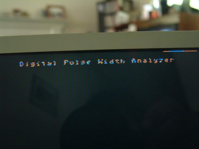
Also, I tried replacing the original delay with NOP's and you can see the result below, why in the heck would it do this? (There is no JSR in the PLTPXL routine because I want it to plot as fast as possible, and this routine is at the heart of my problem. When I figure out this delay problem there will be no JSR's.)

Here's some pics so you can see what's going on. When I call PLTPXL it looks like this:
...
PHA
PHX
JSR PLTPXL
PLX
PLA
...

Thanks for your help!

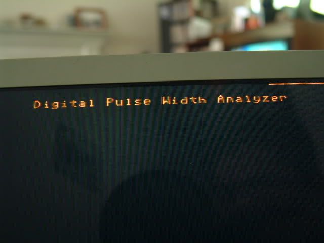
Working:(If I delete the BNE instructions, it still works. If I delete the BNE & DEX instructions, it doesn't work.)
Image
Image

Not working:
Image
Image

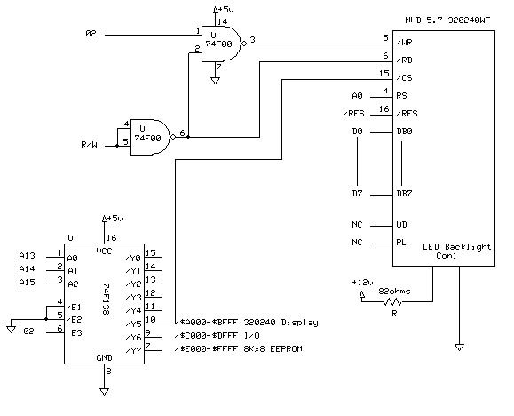
Here's the display interface:
Image
I've tried to use two NAND gates in series with the A0 signal before the display with no change in behavior.


Last edited by ElEctric_EyE on Mon Nov 30, 2009 12:00 pm, edited 1 time in total.

Top
 Profile  
Reply with quote  
 Post subject:
PostPosted: Sun Jul 19, 2009 7:32 pm 
Offline
User avatar

Joined: Fri Aug 30, 2002 1:09 am
Posts: 8543
Location: Southern California
It looks like only the delay between the STAs is relevant, not the one before the first STA. Each delay in your second listing with the NOPs comes to 12 clocks though (2 clocks per NOP), whereas the delays in the first listing only come to 6 clocks each (2 for LDX#, 2 for DEX, and 2 for BNE where the branch is not taken). Too much delay is not usually a problem though.


Top
 Profile  
Reply with quote  
 Post subject:
PostPosted: Sun Jul 19, 2009 9:08 pm 
Offline
User avatar

Joined: Fri Aug 30, 2002 9:02 pm
Posts: 1748
Location: Sacramento, CA
ElEctric_EyE,

I just took a fresh look at the display datasheet and the FSA5606 datasheets.

It appears you are using the 80-series interface. On page 31 of the FSA5606 datasheet, there is an A/C timing diagram. It shows the WRB (X-WR) pin as being the one that goes active last, inactive first. The CSB (X-CS) should be stable first. It does not show the Read mode, but the diagrams on page 20 do.

According to your schematic, the /CS is gated through clk2. your /WR is gated through clk2 but the /RD is not.

Can you try this:

Remove the clk2 to the E3 input of the '138. Add clk2 to the /RD and /WR signals and see if that helps.

That should get your signals to match the datasheet better.

Just a thought....

Daryl


Top
 Profile  
Reply with quote  
 Post subject:
PostPosted: Sun Jul 19, 2009 9:31 pm 
Offline

Joined: Mon Mar 02, 2009 7:27 pm
Posts: 3258
Location: NC, USA
Thanks for checking that 8bit... I chose the 80 series interface over the 6800 series interface because it looked easier. I admit I have a hard time with timing issues. Logic is no problem, but I can't picture the signals in my brain...

Adding 02(phase 2) to the last stage of address decoding adds so many more gates. Your suggestion is not the first time I heard this, (...it is why I chose the 'F' series TTL, still learning here). I was trying to bypass this timing issue with 'F' series "FAST" logic. Going to rewire some things, report back here in abit. Thanks for all your guys help!

_________________
65Org16:https://github.com/ElEctric-EyE/verilog-6502


Top
 Profile  
Reply with quote  
 Post subject:
PostPosted: Sun Jul 19, 2009 10:34 pm 
Offline
User avatar

Joined: Fri Aug 30, 2002 1:09 am
Posts: 8543
Location: Southern California
Sounds similar to the 65c22 VIA, which needs the chip selects to be valid and stable before phase 2 rises, meaning you can't gate the chip selects with phase 2.


Top
 Profile  
Reply with quote  
 Post subject:
PostPosted: Mon Jul 20, 2009 12:39 pm 
Offline

Joined: Mon Mar 02, 2009 7:27 pm
Posts: 3258
Location: NC, USA
I think I misread your post the first time I read it 8bit... I have just tried to just hold e3 high on the '138. The display is getting garbage data... I have enough time this morning to rehook 02 back up and try putting the delay between the STA's as Garth suggested.

edit: Tried the delay in between STA's. Looked like this: LDA,STA,delay.LDA,STA. Also tried increasing the value of x. Didn't work.

Any other ideas?

_________________
65Org16:https://github.com/ElEctric-EyE/verilog-6502


Top
 Profile  
Reply with quote  
 Post subject:
PostPosted: Mon Jul 20, 2009 2:26 pm 
Offline
User avatar

Joined: Fri Aug 30, 2002 9:02 pm
Posts: 1748
Location: Sacramento, CA
ElEctric_EyE wrote:
I think I misread your post the first time I read it 8bit... I have just tried to just hold e3 high on the '138. The display is getting garbage data...


In addition to holding E3 high (which was what I was trying to say, sorry for not being more clear), the /RD and /WR pins both need to be gated with clk2. However, since your code is just performing writes, this should have improved things.

In the original configuration, are you able to perform reads without error?

The datasheet clearly shows the RS being stable first, followed by the /CS, then either /RD or /WR. with /RD or /WR going high first.

A0 (RS) should become stable along with A12-15. The '138 should provide the /CS after its propagation delay (but before clk2 goes high), and the /RD or /WR should go active after the propagation delays with clk2.

There could be an issue with the holding times on the databus after /RD or /WR go inactive. You would need a scope to check that.

If I understand the datasheet correctly, you set up the internal RAM address pointer , then enable writes to RAM, followed by a stream of data write cycles, and end with a "finished" command. Is that correct?

Could you post all of your code used to init and communicate with the display? We might be help more if we had a bigger picture.

Daryl


Top
 Profile  
Reply with quote  
 Post subject:
PostPosted: Mon Jul 20, 2009 10:58 pm 
Offline

Joined: Mon Mar 02, 2009 7:27 pm
Posts: 3258
Location: NC, USA
viewtopic.php?t=1370&start=75
4 posts down I mentioned a small clip from an article by Gene Zumchak from an old Compute! magazine. I copied his 8080 /RD /WR interface, and it incorporates the R/W into 02. Is this correct? I have not tested reading yet...

8 posts down I show the INIT routine which sets up the display in the most basic way, nothing fancy like look up tables..., and also the CLRSCR routine which shows how to write to the display.

Now thinking... You say A0 should become stable along with A13-A15. Do you think my problem is not gating A0 with 02 as I gate A13-A15 with 02 on the '138? ****, I'll bet you that's my problem! I thought there was something up with A0, I originally just tried putting it through 2 NAND gates to delay it. BRB...

_________________
65Org16:https://github.com/ElEctric-EyE/verilog-6502


Top
 Profile  
Reply with quote  
 Post subject:
PostPosted: Mon Jul 20, 2009 11:20 pm 
Offline
User avatar

Joined: Fri Aug 30, 2002 9:02 pm
Posts: 1748
Location: Sacramento, CA
ElEctric_EyE wrote:
Now thinking... You say A0 should become stable along with A13-A15. Do you think my problem is not gating A0 with 02 as I gate A13-A15 with 02 on the '138? ****, I'll bet you that's my problem! I thought there was something up with A0, I originally just tried putting it through 2 NAND gates to delay it. BRB...


No, A0 should not be gated with 02. It will become stable and stay stable for 1/2 of 02 low and all of 02 high.

I'll go back an check the link you referenced tonight.

Daryl


Top
 Profile  
Reply with quote  
 Post subject:
PostPosted: Tue Jul 21, 2009 12:44 pm 
Offline
User avatar

Joined: Fri Aug 30, 2002 9:02 pm
Posts: 1748
Location: Sacramento, CA
ElEctric_EyE,

I reviewed your init code. It looks mostly right out of the manual. Any reason you have the VSYNC (reg 1F) set for 1F vs. 08? If the init code runs without the delays, I don't see why the memory writes should need them. Are you sure the init code is actually modifying registers?

You may want to do a test. Write a non-default value to a register and then read it back to be sure it took. Do several different addresses.

Also, all the datasheets reference this device as having a 3.3v power supply and its inputs do not appear to be 5v tolerant. Can you confirm that? This could be causing a lot of inconsistency.

Daryl


Top
 Profile  
Reply with quote  
 Post subject:
PostPosted: Tue Jul 21, 2009 3:42 pm 
Offline

Joined: Mon Mar 02, 2009 7:27 pm
Posts: 3258
Location: NC, USA
I'll check on the VSYNC value... I have tried to change many settings, The one a had to modify is the rotate register because I unknowingly mounted it upside down when I made the mounts and connections. Without the init routine the screen starts out with multicolored static, so I know all the reg's are being written.

75% of the time the display will boot up properly after a power up. Once in awhile I'll have to reset it a couple times for it to work.

I'll try your suggestion on the write/read from some registers.

There's no mention on the New Haven datasheet about the display being 5V tolerant, however the FSA506 datasheet does say this in chapter 6.1:

"6.1 DC characteristics
DC Characteristics of 3.3V with 5V Tolerance I/O Cells"

Since the circuit board only contains that one chip I assumed that it is 5V tolerant, except the /res. But that is only pulsed quickly so I'm not worried about overloading that line.

Well if we can't figure out this problem, I will have to assume there was a problem inherent in the design and that is why they stopped selling it right after I bought it.

A few other notes though. They still have an app note for the 8 bit version. I don't know the language it is written in but I see there is a delay definition in the code, which is why I started experimenting with delays in the first place. Here's the link:
http://www.newhavendisplay.com/app_note ... 6_8bit.txt

Maybe someone can interpret it.

Also, this display is supposed to have 256K colors, which is 18bit data, which means I would have to send 3 consecutive 8bit data. When I try that it looks screwy.

It seems I have only 65K colors, sending 2 consecutive 8bit data works.
_________________
65Org16:https://github.com/ElEctric-EyE/verilog-6502


Top
 Profile  
Reply with quote  
 Post subject:
PostPosted: Wed Jul 22, 2009 1:25 am 
Offline

Joined: Wed Jul 22, 2009 1:05 am
Posts: 1
I used the same display in one of my new designs (prototype), and it works quite well. New Haven did remove it from the site, but we bought another one by calling them directly. There is also another company that produces the same display. It never displayed the data I sent to it improperly, ever. The display is driven from one of the ports, so it runs at about 2-3MHz (peak). The uC I am using is a Freescale 9S12 (68HC12) running at 16MHz (for now). I use a few 74LVCC3245 devices to interface the 5V bus to the 3.3V bus. The display can show up to 65536 colors, which is really enough since the interface is only 8-bit.

Image


Top
 Profile  
Reply with quote  
Display posts from previous:  Sort by  
Post new topic Reply to topic  [ 297 posts ]  Go to page Previous  1 ... 4, 5, 6, 7, 8, 9, 10 ... 20  Next

All times are UTC


Who is online

Users browsing this forum: No registered users and 33 guests


You cannot post new topics in this forum
You cannot reply to topics in this forum
You cannot edit your posts in this forum
You cannot delete your posts in this forum
You cannot post attachments in this forum

Search for:
Jump to: