BigDumbDinosaur wrote:
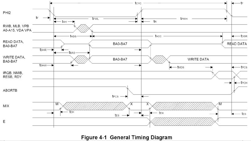
Although the timing diagram implies that RDY can be asserted at any time, I was told that the MPU's behavior is undefined if RDY is asserted when Ø2 is low and hence the bank address may not be valid.
Interesting if the behaviour is indeed undefined, and perhaps a little inconvenient.
BigDumbDinosaur wrote:
I believe that any design that asserts/de-asserts RDY on the rise of Ø2 should work as expected.
Your rule is stricter than mine, and if we've reason to doubt then following that rule would be safe. Someday I might be a position to investigate the behaviour of parts I have, and I could prove myself wrong. I couldn't show I was right, if the behaviour is not defined.
The thing is, I haven't seen the ambiguity in the datasheet which you saw.
It's certainly true that if RDY is not sampled, but just modifies the internal clocking combinatorially, modifying it during PHI1 might cause the role of the databus to switch between data and address. And it's true that if it is sampled, its value outside the setup+hold window can't change the behaviour of the device.
I think neither of us have experimental evidence either way - just possibly André has seen something, except he describes modifying RDY during PHI2, which both of us think should be fine.


