6502.org Forum  Projects  Code  Documents  Tools  Forum
It is currently Fri Nov 22, 2024 7:20 am

All times are UTC


Post new topic Reply to topic  [ 150 posts ]  Go to page Previous  1 ... 5, 6, 7, 8, 9, 10  Next
Author Message
 Post subject: PLCC WW sockets
PostPosted: Mon Apr 26, 2021 5:26 am 
Offline
User avatar

Joined: Sat Sep 29, 2012 10:15 pm
Posts: 904
GARTHWILSON wrote:
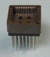
Ok, I took a picture of one of mine, a 44-pin, from Aries (although they no longer supply it):
Image
...


Do you by any chance have the pinout spec for these sockets? I am more interested in PLCC-28, actually, for 22V10s

Thanks

_________________
In theory, there is no difference between theory and practice. In practice, there is. ...Jan van de Snepscheut


Top
 Profile  
Reply with quote  
 Post subject: Re: PLCC WW sockets
PostPosted: Mon Apr 26, 2021 6:13 am 
Offline
User avatar

Joined: Fri Aug 30, 2002 1:09 am
Posts: 8543
Location: Southern California
enso wrote:
Do you by any chance have the pinout spec for these sockets? I am more interested in PLCC-28, actually, for 22V10s

Ok, I checked one with the DMM continuity-check function, and drew this. It's a top view. The contacts to the IC are shown farther out than they should be, just so there would be room to draw the connections.


Attachments:
PLCC28WWsocketPinout.gif
PLCC28WWsocketPinout.gif [ 17.57 KiB | Viewed 40527 times ]

_________________
http://WilsonMinesCo.com/ lots of 6502 resources
The "second front page" is http://wilsonminesco.com/links.html .
What's an additional VIA among friends, anyhow?
Top
 Profile  
Reply with quote  
 Post subject: Re: PLCC WW sockets
PostPosted: Mon Apr 26, 2021 5:24 pm 
Offline
User avatar

Joined: Sat Sep 29, 2012 10:15 pm
Posts: 904
GARTHWILSON wrote:
Ok, I checked one with the DMM continuity-check function, and drew this. It's a top view. The contacts to the IC are shown farther out than they should be, just so there would be room to draw the connections.

I feel embarrassed... I could've done that myself :oops: but was too lazy after spending what felt like an hour on octopart... I thought you probably have a specsheet somewhere. Thank you.

_________________
In theory, there is no difference between theory and practice. In practice, there is. ...Jan van de Snepscheut


Top
 Profile  
Reply with quote  
 Post subject: DIY WW sockets
PostPosted: Mon Apr 26, 2021 7:30 pm 
Offline
User avatar

Joined: Sat Sep 29, 2012 10:15 pm
Posts: 904
Good news!

It is feasible to 3d-print your own wire-wrap sockets.

As previously discussed, wire-wrap sockets have gotten expensive and hard to get, especially when it comes to PLCCs. But for those of us with inexpensive (mine was under $200) 3D-printers, there is another option: print your own socket. Here is a picture of my early experiments:
Attachment:
DSCF2785.1.JPG
DSCF2785.1.JPG [ 230.25 KiB | Viewed 40501 times ]

Shown: a few DIP sockets, a pinned ̶P̶L̶C̶C̶-̶2̶8̶ PGA-28 socket (all but last pin, shown next to it), and an unpinned P̶L̶C̶C̶-̶2̶8̶PGA-28 socket.

_________________
In theory, there is no difference between theory and practice. In practice, there is. ...Jan van de Snepscheut


Last edited by enso on Mon Apr 26, 2021 7:42 pm, edited 1 time in total.

Top
 Profile  
Reply with quote  
PostPosted: Mon Apr 26, 2021 7:40 pm 
Offline
User avatar

Joined: Fri Aug 30, 2002 1:09 am
Posts: 8543
Location: Southern California
I'd say that what you have there is a PGA (pin grid array) socket, and you'll plug a thru-hole PLCC socket into it.

_________________
http://WilsonMinesCo.com/ lots of 6502 resources
The "second front page" is http://wilsonminesco.com/links.html .
What's an additional VIA among friends, anyhow?


Top
 Profile  
Reply with quote  
PostPosted: Thu May 06, 2021 7:29 pm 
Offline
User avatar

Joined: Sat Sep 29, 2012 10:15 pm
Posts: 904
I've spent the last couple of weeks blowing my mind and really trying to figure out how circuits work. It's amazing how incredibly ignorant I've been all my life! You did try to straighten out my primitive thinking, but what really did it was watching Rick Hartley's videos, in particular 'How to Achieve Proper Grounding' https://www.youtube.com/watch?v=ySuUZEjARPY. But all of his videos are extremely enlightening, and unlike many youtubers he does not waste your time with self-aggrandizing crap.

The most important points I wish I had understood earlier:
  • Clock speed is irrelevant; frequencies implied by rise time decide the 'speed' of the circuit. These are pre-decided by the chips used; the clock only triggers your high-speed circuit every so often.
  • Energy in a circuit is not in the copper wiring; it is a field in the dielectric substrate between the conductor and the lowest-impedance return. The copper acts as a waveguide, directing the flow of energy along a path.
  • Controlling impedance.. capacitance and inductance of interconnects at different frequencies, etc,
  • Plan the return path - it is at least as important as the forward path, and may bite you if an unexpected lower impedance path exists (such as a nearby signal or power conductor)

I feel enlightened and horrified. I've been blindly playing 'connect-the-dots' in my PCB design, with a vague understanding that somehow a 'good ground' was important. I can see now that many of my signal tracks with no obvious returns created ridiculous fields that coupled to everything in their way to the nearest low-impedance return path. And I see why having a ground-plane is a pretty good idea, and why copper pours are not at all a substitute. I thank everyone who tried to tell me...

_________________
In theory, there is no difference between theory and practice. In practice, there is. ...Jan van de Snepscheut


Last edited by enso on Thu May 06, 2021 8:12 pm, edited 2 times in total.

Top
 Profile  
Reply with quote  
PostPosted: Thu May 06, 2021 7:44 pm 
Offline
User avatar

Joined: Thu Dec 11, 2008 1:28 pm
Posts: 10985
Location: England
Thanks for the pointer!


Top
 Profile  
Reply with quote  
PostPosted: Sat Feb 19, 2022 9:56 am 
Offline
User avatar

Joined: Fri Aug 30, 2002 1:09 am
Posts: 8543
Location: Southern California
Since someone just asked me about VDD and trace width on a 2-layer board, I did another search for an online calculator for this, ie, basically a flat wire, and found this. For situations where someone does not feel like they can afford a multilayer board, so they try for just a 2-layer, we frequently see recommendations to make the power traces super wide. This has been very much overemphasized and misunderstood. Resistance is not the problem, and an .008"-wide trace can handle 500mA with ease. The real enemy is inductance, and making a trace wider on a 2-layer board with no ground plane has very little effect on its inductance. Doubling the width of a 2"-long trace on 1oz copper, from .010" to .020", only brings the inductance down about 10%; IOW, it has almost no effect. Wanna go wider? If we widen it from .010" to .050", ie, multiplying the width by five, the reduction in inductance is not even 25%. Bypass capacitors at each IC will reduce the need to minimize VDD trace inductance anyway, and the ground connections will handle much of the signals' return currents.

So if you're limited to two layers, it might be best to route a nice, fine grid of ground connections, so there's the least impedance from the ground pin of any one IC to the ground pin of another IC, then get the bypass capacitors connected with the shortest practicable connections from each IC's VDD pin to its ground pin (which might mean putting them on the back of the board, under the IC). Then route all the signals, and then sew-in a VDD grid with the room that's left. An autorouter won't have the intelligence to do a very good job at that; so I would do the ground and VDD connections by hand.

_________________
http://WilsonMinesCo.com/ lots of 6502 resources
The "second front page" is http://wilsonminesco.com/links.html .
What's an additional VIA among friends, anyhow?


Top
 Profile  
Reply with quote  
PostPosted: Sat Feb 19, 2022 4:20 pm 
Offline
User avatar

Joined: Sun Jun 30, 2013 10:26 pm
Posts: 1949
Location: Sacramento, CA, USA
I don't know if automotive technology is an appropriate branch of this discussion, but in my decades of experience with engine control systems I have found that a "dirty" or "noisy" VDD can be just as vexing as a "dirty" or "noisy" VSS. I don't design PCBs, but if I did I would treat them with equal significance wherever and whenever possible.

_________________
Got a kilobyte lying fallow in your 65xx's memory map? Sprinkle some VTL02C on it and see how it grows on you!

Mike B. (about me) (learning how to github)


Top
 Profile  
Reply with quote  
PostPosted: Sat Feb 19, 2022 5:10 pm 
Offline

Joined: Fri Dec 21, 2018 1:05 am
Posts: 1117
Location: Albuquerque NM USA
I used autorouter extensively. My designs were always 2-layer PCB up til few months ago. My 2-layer design approach is reducing board outline by 0.05" all around and bring out several power/ground pads to the edge of the reduced board outline; run the autorouter and then increase the board outline by 0.05" and manually route 0.025" power and ground traces connecting to the edge power/ground pads. This is an easy way to provide multiple ground returns.

W65C02/816 plus fast RAM are noisy combination. for 4"x4" size boards with W65C02 & RAM I'm gravitating toward 4-layer pc board. I've also found dynamic RAM can be quite noisy so I'm now migrating my designs with DRAM memories to 4-layer PCB.
Bill


Top
 Profile  
Reply with quote  
PostPosted: Sat Feb 19, 2022 11:23 pm 
Offline
User avatar

Joined: Fri Aug 30, 2002 1:09 am
Posts: 8543
Location: Southern California
barrym95838 wrote:
I don't know if automotive technology is an appropriate branch of this discussion, but in my decades of experience with engine control systems I have found that a "dirty" or "noisy" VDD can be just as vexing as a "dirty" or "noisy" VSS. I don't design PCBs, but if I did I would treat them with equal significance wherever and whenever possible.

True; but if you have the bypass capacitors well placed, VDD will become another ground as far as AC is concerned, so it won't be any noisier than VSS.

My point however was that making 2-layer boards' traces wider does not significantly reduce their inductance or the resulting problems. Wider traces just take more board space, making it harder to route the signals; and then to get them all in, you might just have to put components farther apart, which just makes the board bigger, which in turn increases connection lengths, which increases the traces' inductance—so there's no benefit.

_________________
http://WilsonMinesCo.com/ lots of 6502 resources
The "second front page" is http://wilsonminesco.com/links.html .
What's an additional VIA among friends, anyhow?


Top
 Profile  
Reply with quote  
PostPosted: Sun Feb 20, 2022 1:42 am 
Offline
User avatar

Joined: Fri Dec 11, 2009 3:50 pm
Posts: 3367
Location: Ontario, Canada
Just to elaborate on Garth's post above and his second paragraph here ...

Because making PCB traces traces wider does not significantly reduce their inductance, even thin traces are acceptable for creating a grid of ground traces (as an approximation of an actual ground plane). And thin traces mean such a grid needn't add significant area to the board.

Neither would the grid complicate the routing much. Regarding signal wiring, it's generally true that north-south traces tend to go on one side of the board and east-west traces on the other. And the ground grid can "go with the flow" of whatever else is there, interleaving its north-south ground traces with north-south signal traces, and likewise for east-west.

At every point where a N-S ground trace crosses an E-W ground trace you'll want to connect the two (otherwise the grid doesn't approximate a plane -- current must be able to flow N-S, E-W or in a zigzag for diagonal travel). And if the N-S and E-W ground traces are on opposite sides of the board then you'll need to use a via to connect them. Vias do add a bit of inductance, but hardly enough to negate the benefit of the grid.

I'm not advocating grids as the answer to every situation. But they certainly bear consideration as one useful option on the continuum between outright rats-nests and rigorous, controlled-impedance designs. As a moderately interesting data point, it's worth noting that portions of my 1988 KK Computer use 74AC series logic running at 80 MHz. KK is implemented in wire-wrap, and there's no ground plane. But there is a ground grid, which in this case means almost every IC has four connections (N, S, E and W) emanating from its Gnd pin to those of its neighbors. (Also, almost every IC's Gnd pin has a bypass cap running directy to the IC's Vcc pin, just as Garth suggested in the linked post).

-- Jeff
_________________
In 1988 my 65C02 got six new registers and 44 new full-speed instructions!
https://laughtonelectronics.com/Arcana/ ... mmary.html


Top
 Profile  
Reply with quote  
PostPosted: Sun Jul 03, 2022 5:29 am 
Offline
User avatar

Joined: Fri Aug 30, 2002 1:09 am
Posts: 8543
Location: Southern California
enso wrote:
I've spent the last couple of weeks blowing my mind and really trying to figure out how circuits work. It's amazing how incredibly ignorant I've been all my life! You did try to straighten out my primitive thinking, but what really did it was watching Rick Hartley's videos, in particular 'How to Achieve Proper Grounding' https://www.youtube.com/watch?v=ySuUZEjARPY. But all of his videos are extremely enlightening, and unlike many youtubers he does not waste your time with self-aggrandizing crap.

The most important points I wish I had understood earlier:
  • Clock speed is irrelevant; frequencies implied by rise time decide the 'speed' of the circuit. These are pre-decided by the chips used; the clock only triggers your high-speed circuit every so often.
  • Energy in a circuit is not in the copper wiring; it is a field in the dielectric substrate between the conductor and the lowest-impedance return. The copper acts as a waveguide, directing the flow of energy along a path.
  • Controlling impedance.. capacitance and inductance of interconnects at different frequencies, etc,
  • Plan the return path - it is at least as important as the forward path, and may bite you if an unexpected lower impedance path exists (such as a nearby signal or power conductor)

I feel enlightened and horrified. I've been blindly playing 'connect-the-dots' in my PCB design, with a vague understanding that somehow a 'good ground' was important. I can see now that many of my signal tracks with no obvious returns created ridiculous fields that coupled to everything in their way to the nearest low-impedance return path. And I see why having a ground-plane is a pretty good idea, and why copper pours are not at all a substitute. I thank everyone who tried to tell me...

Yeah, Rick Hartley is really good, along with Eric Bogatin and Suzie Web.

enso wrote:
GARTHWILSON wrote:
Ok, I checked one with the DMM continuity-check function, and drew this. It's a top view. The contacts to the IC are shown farther out than they should be, just so there would be room to draw the connections.

I feel embarrassed... I could've done that myself :oops: but was too lazy after spending what felt like an hour on octopart... I thought you probably have a specsheet somewhere. Thank you.

I've looked at the data sheets for several different brands of these, and they're not the clearest on whether they all agree. Some data sheets don't give the pinout at all, and others don't tell you if it's a top view or bottom view. It's probably a top view; but they don't say. Do you know these things? If you make a board for one brand of TH PLCC sockets and then later have to get a different brand, is there any danger you'll suddenly have the wrong pinout?

I'm laying out an '816 board. I thought of just soldering PLCCs directly to the board, but I would need space around them to solder them, meaning sockets wouldn't take any more room. Thru-hole sockets kind of precludes putting parts on both sides of the board right there, but SMT sockets cannot be hand-soldered. I'm also staying away from parts so small I'm not sure I could finish a board and not have soldering defects, so I don't think I want to try the PQFPs for this.

_________________
http://WilsonMinesCo.com/ lots of 6502 resources
The "second front page" is http://wilsonminesco.com/links.html .
What's an additional VIA among friends, anyhow?


Top
 Profile  
Reply with quote  
PostPosted: Sun Jul 03, 2022 6:01 am 
Offline
User avatar

Joined: Thu May 28, 2009 9:46 pm
Posts: 8505
Location: Midwestern USA
GARTHWILSON wrote:
I've looked at the data sheets for several different brands of these, and they're not the clearest on whether they all agree. Some data sheets don't give the pinout at all, and others don't tell you if it's a top view or bottom view. It's probably a top view; but they don't say. Do you know these things? If you make a board for one brand of TH PLCC sockets and then later have to get a different brand, is there any danger you'll suddenly have the wrong pinout?

There are JEDEC standards for through-hole PLCC sockets that include pin numbering, pin position and external dimensions. In my POC units, I’ve used several different brands of sockets and have never had any kind of interchangeability issue.

Quote:
I thought of just soldering PLCCs directly to the board, but I would need space around them to solder them, meaning sockets wouldn't take any more room.

I went through that exercise when I was laying out POC V1.3 and came to the same conclusion. So, I’ve stuck with sockets.

Quote:
Thru-hole sockets kind of precludes putting parts on both sides of the board right there, but SMT sockets cannot be hand-soldered. I'm also staying away from parts so small I'm not sure I could finish a board and not have soldering defects, so I don't think I want to try the PQFPs for this.

Realistically, the smaller pitches are best handled with reflowing, which means solder paste and a stencil.

_________________
x86?  We ain't got no x86.  We don't NEED no stinking x86!


Top
 Profile  
Reply with quote  
PostPosted: Sun Jul 03, 2022 6:36 am 
Offline
User avatar

Joined: Fri Aug 30, 2002 1:09 am
Posts: 8543
Location: Southern California
Thanks for the reassurance. I just made my 44-pin PLCC socket PCB components. I'll see how the room compares and decide if I want to solder the PLCCs to the board directly, or socket them. I expect sockets will win, in spite of the extra inductance and the fact that they take room on every layer.

_________________
http://WilsonMinesCo.com/ lots of 6502 resources
The "second front page" is http://wilsonminesco.com/links.html .
What's an additional VIA among friends, anyhow?


Top
 Profile  
Reply with quote  
Display posts from previous:  Sort by  
Post new topic Reply to topic  [ 150 posts ]  Go to page Previous  1 ... 5, 6, 7, 8, 9, 10  Next

All times are UTC


Who is online

Users browsing this forum: No registered users and 19 guests


You cannot post new topics in this forum
You cannot reply to topics in this forum
You cannot edit your posts in this forum
You cannot delete your posts in this forum
You cannot post attachments in this forum

Search for:
Jump to: