6502.org Forum  Projects  Code  Documents  Tools  Forum
It is currently Sat Sep 21, 2024 5:43 am

All times are UTC


Post new topic Reply to topic  [ 9 posts ] 
Author Message
PostPosted: Mon Feb 22, 2021 9:56 pm 
Offline
User avatar

Joined: Wed Aug 17, 2005 12:07 am
Posts: 1228
Location: Soddy-Daisy, TN USA
So while designing my next SBC, I'm taking a lot of inspiration from the VIC-20 (and Apple II).

One thing that is puzzling to me is how they are using two different VIA pins to drive the same serial pin on the port.

I have attached the PDF schematic and a cut-away I did illustrating what I am talking about.

On the serial port, pin 5 is for IN/OUT serial data. For serial data OUT (from VIA to port) it uses CB2 on the first VIA. For serial IN (from port to VIA) it uses PA3 on another VIA. You can see there is an inverter used along with a pull-up resistor.

So my question is, how in the world does this work? LOL

Any clues would be appreciated.

Thanks.


Attachments:
n_schematic.pdf [696.21 KiB]
Downloaded 30 times
File comment: Highlighted Section
VIC-20_Serial.PNG
VIC-20_Serial.PNG [ 135.77 KiB | Viewed 676 times ]

_________________
Cat; the other white meat.
Top
 Profile  
Reply with quote  
PostPosted: Mon Feb 22, 2021 10:14 pm 
Offline
User avatar

Joined: Thu Dec 11, 2008 1:28 pm
Posts: 10938
Location: England
That's no ordinary inverter - that's open-collector.


Top
 Profile  
Reply with quote  
PostPosted: Tue Feb 23, 2021 7:43 am 
Offline

Joined: Tue Sep 03, 2002 12:58 pm
Posts: 325
The C64 has the same arrangement. The easiest way to have multiple devices on the same bus, with no possibility of conflict, is to use open collector drivers. Any device can pull the signal low, and if none do, the resistor pulls it high. If two devices pull it low at the same time, no harm is done (whatever data you're transmitting will get corrupted, but there won't be any physical damage).
VIAs don't have open collector outputs, so you need something like the 7406. But that can't change direction. The solution they've gone with is to use two VIA pins: one is always output and drives the 7406, the other is always input and samples whatever is on that line, wherever it came from.


Top
 Profile  
Reply with quote  
PostPosted: Tue Feb 23, 2021 7:56 am 
Offline
User avatar

Joined: Fri Nov 09, 2012 5:54 pm
Posts: 1429
CB2 is configurated as an output, driving a 7406 inverter which switches the voltage at the R19 pullup resistor to GND.
PA1 is configurated as an input, sensing the voltage at R19.

Hmm... in that schematic, R19 is tied to '+15', and I think that's a typo and it should be '+5V'.
A 7406 output can take 30V, but a 6522 isn't meant to survive +15V on an I\O pin.
Anyhow, the VIC-20 power supply doesn't provide +15V.

In the original VIC-20 schematics, this resistor is tied to +5V.
Maybe somebody should try to contact the author of that PDF.


Top
 Profile  
Reply with quote  
PostPosted: Tue Feb 23, 2021 8:48 am 
Offline
User avatar

Joined: Fri Aug 30, 2002 1:09 am
Posts: 8510
Location: Southern California
John West wrote:
VIAs don't have open collector outputs, so you need something like the 7406.

Ah, but they can! :D What you do is set the output-register bit to 0, and then change the bit in the data-direction register. When you want to pull the pin low, you make it an output. If you want to let it float high (or just be pulled low by something else), make it an input. Then you can read it too. I've done this for I²C.

_________________
http://WilsonMinesCo.com/ lots of 6502 resources
The "second front page" is http://wilsonminesco.com/links.html .
What's an additional VIA among friends, anyhow?


Top
 Profile  
Reply with quote  
PostPosted: Tue Feb 23, 2021 10:51 am 
Offline
User avatar

Joined: Fri Nov 09, 2012 5:54 pm
Posts: 1429
Nowaday a 5V powered W65C22 I/O pin can sink 3.2mA min. to GND (PDF page 38).
An old NMOS 6522 (1977) I/O pin can only sink 1.6mA min. to GND (PDF page 21).
74LS06 output can sink 40mA to GND (PDF page 4).

Means when a NMOS 6522 I/O pin can only sink 1.6mA to GND, a pullup resistor to +5V needs to have at least 3.125kOhm.
//Higher impedance also means lower frequency because of all the capacitances on a signal line.

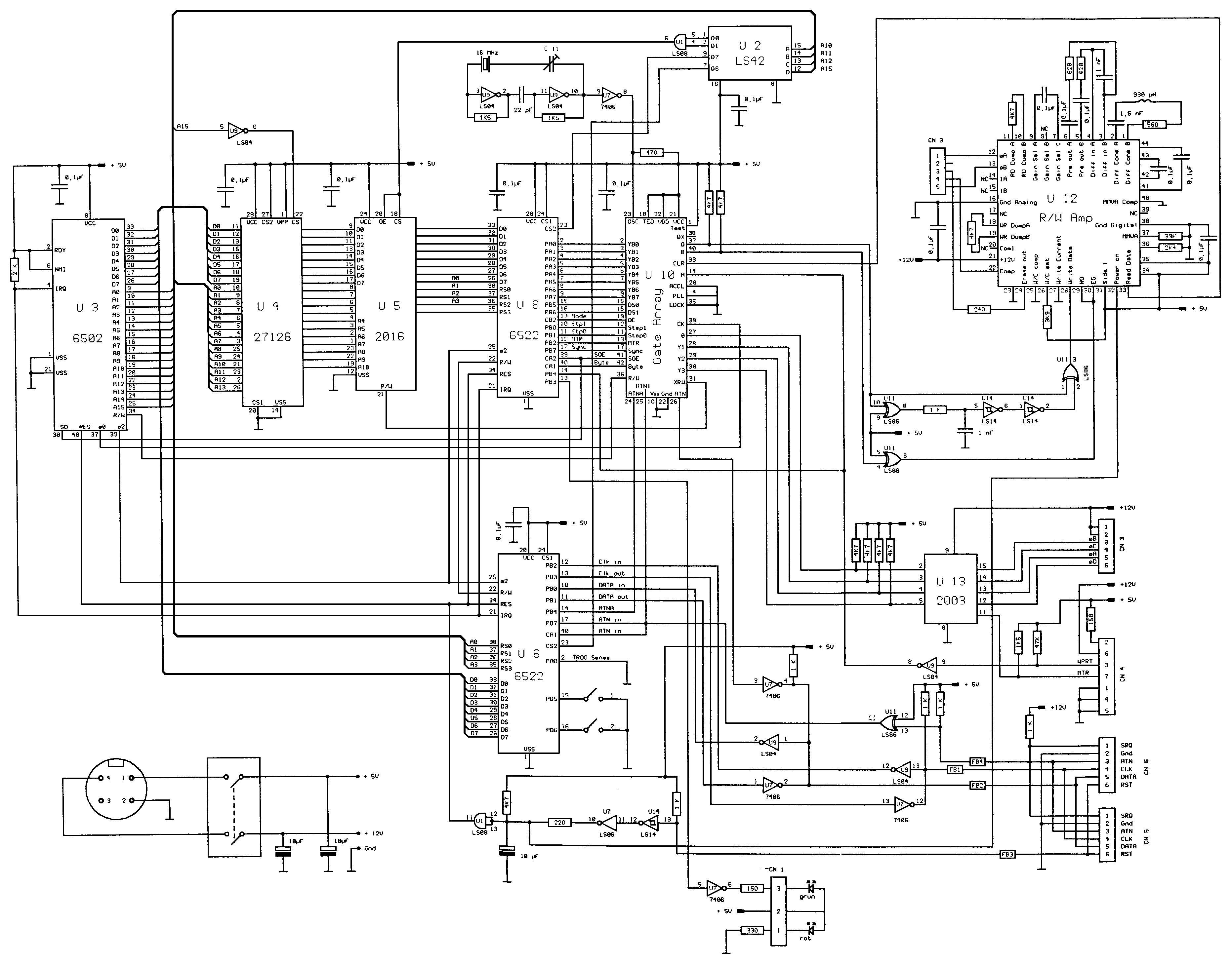
When taking a look at the 1541-II schematics,
it appears that the peripherals for the serial IEC bus have 1kOhm pullup resistors on the signal lines, too.

This means you need to sink 5mA to GND on a IEC bus signal line only for the VIC-20 itself,
plus another 5mA for every peripheral device which is plugged to the bus.

VIC-20 plus 1541 drive would be 10mA in total, and even for a modern W65C22 that's too much.

74LS06 can sink up to 40mA to GND, so in theory using 74LS06 as a line driver would allow plugging up to 7 peripherals to the VIC-20 IEC bus.


Top
 Profile  
Reply with quote  
PostPosted: Tue Feb 23, 2021 5:11 pm 
Offline
User avatar

Joined: Fri Aug 30, 2002 1:09 am
Posts: 8510
Location: Southern California
ttlworks wrote:
Nowadays a 5V powered W65C22 I/O pin can sink 3.2mA min. to GND (PDF page 38).

The truth is much, much better than the data sheet lets on. In my own tests, the W65C02S can pull within 0.8V of either rail (yes, even pulling up) with a 220-ohm load, which means 19mA; and if you just dead-short it, you'll get 50mA.

_________________
http://WilsonMinesCo.com/ lots of 6502 resources
The "second front page" is http://wilsonminesco.com/links.html .
What's an additional VIA among friends, anyhow?


Top
 Profile  
Reply with quote  
PostPosted: Wed Feb 24, 2021 6:29 am 
Offline
User avatar

Joined: Fri Nov 09, 2012 5:54 pm
Posts: 1429
Garth, since the parameters in the WDC datasheets tend to be somewhat conservative this was to be expected, and I believe you, of course.

But since WDC is a fabless semiconductor company, it's an interesting question if it would affect the real_life electrical parameters of W65C02 chips
if the production of the silicon (hypothetically) might be moved to another foundry someday.

So I can't just ignore the specifications in the official WDC datasheets. :)


Top
 Profile  
Reply with quote  
PostPosted: Wed Feb 24, 2021 7:32 am 
Offline
User avatar

Joined: Fri Aug 30, 2002 1:09 am
Posts: 8510
Location: Southern California
ttlworks wrote:
since WDC is a fabless semiconductor company, it's an interesting question if it would affect the real-life electrical parameters of W65C02 chips if the production of the silicon (hypothetically) might be moved to another foundry someday.

So I can't just ignore the specifications in the official WDC datasheets.
:)

True; they don't guarantee such high-current capability. We'll always have to test certain things for ourselves if we want to know the real limits; although if WDC specifies the masks (which I expect is kind of like supplying gerber files for a PCB), I don't think the output current capability will be decreasing as technology advances. I wonder how many years they go between production runs.

_________________
http://WilsonMinesCo.com/ lots of 6502 resources
The "second front page" is http://wilsonminesco.com/links.html .
What's an additional VIA among friends, anyhow?


Top
 Profile  
Reply with quote  
Display posts from previous:  Sort by  
Post new topic Reply to topic  [ 9 posts ] 

All times are UTC


Who is online

Users browsing this forum: Google [Bot] and 20 guests


You cannot post new topics in this forum
You cannot reply to topics in this forum
You cannot edit your posts in this forum
You cannot delete your posts in this forum
You cannot post attachments in this forum

Search for:
Jump to: