6502.org Forum  Projects  Code  Documents  Tools  Forum
It is currently Sat Nov 23, 2024 1:40 am

All times are UTC


Post new topic Reply to topic  [ 182 posts ]  Go to page Previous  1 ... 3, 4, 5, 6, 7, 8, 9 ... 13  Next
Author Message
PostPosted: Wed Oct 28, 2020 1:15 am 
Offline
User avatar

Joined: Sun Oct 18, 2015 11:02 pm
Posts: 428
Location: Toronto, ON
joanlluch wrote:
I think this only works (possibly) because the 6502 uses two cycles anyway to complete instructions. So in fact you have a two step gap between the fetch-decode-execute-writeback sequence of one cycle to the next. Or in other words, the next instruction fetch happens while the current cycle is in the executing stage, not while it is in the decode stage, as it would be the case for a standard pipelined risc processor. Is this right, or I am missing something fundamental here?
Very astute observation Joan. There is a “gap”, but here is perhaps a more general way to think about this:

The pipeline always fetches and executes one microinstruction per cycle. We avoid WRITEBACK data hazards by ensuring that there is an intervening microinstruction between a register read in the DECODE stage and a corresponding register write in the WRITEBACK stage. On a 6502 multi-cycle implementation, a register write operation is always followed by an operand-fetch for the next instruction (or a nop if the next instruction is a single-byte instruction). Hence, data hazards never occur.

In a RISC implementation, it might be useful to think of this intervening microinstruction as a “data delay slot” which can be “filled” to avoid a stall. You can dispense with hardware hazard checks by having the compiler (or some other mechanism) fill these slots ahead of time, either with other instructions in the program, or with nops that resolve the data hazard but do not preform any useful work.

_________________
C74-6502 Website: https://c74project.com


Last edited by Drass on Wed Oct 28, 2020 3:25 am, edited 1 time in total.

Top
 Profile  
Reply with quote  
PostPosted: Wed Oct 28, 2020 1:35 am 
Offline
User avatar

Joined: Sun Oct 18, 2015 11:02 pm
Posts: 428
Location: Toronto, ON
ttlworks wrote:
Now this gives me quite a headache.
You and me both! :)

Quote:
Drass, since the ALU input latches will be edge triggered 74AUC16374 chips or such...
have you considered building the registers with transparent latches like 74AUC16373 ?
BigEd suggested a reference to this in an earlier post. We can use a latch to balance the workload between two stages. This works well if you have a stage that is shorter than the cycle and one that is longer than the cycle but the aggregate is shorter than twice the cycle. In that case, a transparent latch between the stages can be used “borrow” time by having the data flow between the stages as soon as it is ready, rather than only when the clock edge arrives.

In this case, most stages are very well balanced already so there is no “short” stage to borrow from. One possible exception is the BranchTest operation. I am still working that out, but we may benefit from a transparent latch for the flags and/or IR (BranchTest requires the opcode to decide which flags to test. The opcode comes from memory in the prior cycle and gets to the IR 1.5ns early since there is no setup time required).

_________________
C74-6502 Website: https://c74project.com


Last edited by Drass on Wed Oct 28, 2020 4:45 am, edited 3 times in total.

Top
 Profile  
Reply with quote  
PostPosted: Wed Oct 28, 2020 1:48 am 
Offline
User avatar

Joined: Sun Oct 18, 2015 11:02 pm
Posts: 428
Location: Toronto, ON
BigEd wrote:
On the face of it, computing Z should be no worse than a carry-chain problem, and indeed the inputs to the Z function arrive earliest from the LSB and latest from the MSB, so Z might only need to be a gate-delay behind C. (I say this, knowing that computing Z often does seem to be a time-consuming thing. So I'm interested in why the difference between theory and common practice.)
That makes sense. (Or is it concurrent with C? The carry chain requires an additional gate after the MSB of the result, no?)

I wonder if there is any way to optimize the V flag. It requires the MSB of the result IIRC (which admittedly still emerges from the adder before the final carry. So there is that).

_________________
C74-6502 Website: https://c74project.com


Top
 Profile  
Reply with quote  
PostPosted: Wed Oct 28, 2020 3:21 am 
Offline
User avatar

Joined: Sun Oct 18, 2015 11:02 pm
Posts: 428
Location: Toronto, ON
joanlluch wrote:
Thus it also looks to me that just half a cycle for write-back might not be enough time for what's required, and that as Dieter suggests, we might need to allow some incursion onto the second half of the cycle to make this affordable.
Flag evaluation from the C74-6502:
Attachment:
754C39E0-2428-4A58-A943-758C4AFFC8C9.jpeg
754C39E0-2428-4A58-A943-758C4AFFC8C9.jpeg [ 556 KiB | Viewed 1380 times ]
It should fit in a half cycle using CBTLV and NC7SV logic.

_________________
C74-6502 Website: https://c74project.com


Top
 Profile  
Reply with quote  
PostPosted: Wed Oct 28, 2020 6:36 am 
Offline
User avatar

Joined: Thu Apr 11, 2019 7:22 am
Posts: 40
Drass wrote:
BigEd wrote:
On the face of it, computing Z should be no worse than a carry-chain problem, and indeed the inputs to the Z function arrive earliest from the LSB and latest from the MSB, so Z might only need to be a gate-delay behind C. (I say this, knowing that computing Z often does seem to be a time-consuming thing. So I'm interested in why the difference between theory and common practice.)
That makes sense. (Or is it concurrent with C? The carry chain requires an additional gate after the MSB of the result, no?)

I wonder if there is any way to optimize the V flag. It requires the MSB of the result IIRC (which admittedly still emerges from the adder before the final carry. So there is that).

Actually, using a carry look ahead circuitry you can get the C flag at least two gate delays ahead of the result [I mean that we get C before the result, I'm having some use of English trouble with the word 'ahead']. Also you can get the V flag concurrently with the result.

To illustrate it, you can Look at this Logisim Model of my "ALUCore" https://github.com/John-Lluch/CPU74/blob/master/Docs/LogisimDocsV10/ALUCore.png. This is no less and no more than the Dieter multiplexed ALU http://www.6502.org/users/dieter/a2/a2_1.htm with two levels of carry-lookahead, as seen for the 74xx181 / 74xx182 combinations http://www.6502.org/users/dieter/a7/a7_3.htm, with the difference that the carry look ahead goes up to Cn+4 instead of only to Cn+3

- The C flag is generated from the second level carry-lookahead circuit, it is shown on the top right of the drawing. Forget about the "SHR Cy" ic for now, and think that the Carry bit emerges from the 'C4' output of the top right cy-look-ahead ic. Thus the final carry is available before the first level look-aheads provide their carry signals to the end Xor gates, and the Xor gates process them, so that's more than 2 gate delays earlier than the result is available.

- The V flag is generated by Xorting the final Carry with the Carry of the previous bit. The later emerges from the first level carry-lookahead circuit at the bottom right of the drawing, it is depicted as 'Cx' in the logisim model. Thus the Cx is available one gate delay earlier than the Result. Then it is compared (not shown in that drawing) with the final carry by means of a Xor gate, which executes concurrently with the end Xor gates of the adder. Therefore we have the V flag at the same time than the result.

- The problematic flag is still (and surprisingly) the Z flag, which must be computed after the Result

Top
 Profile  
Reply with quote  
PostPosted: Wed Oct 28, 2020 7:20 am 
Offline
User avatar

Joined: Fri Nov 09, 2012 5:54 pm
Posts: 1431
Joan, thanks for the summary.

For address calculations, we would be going to need a temporary carry flag (not visible to the "end user")
which needs to be updated at the end of the ALU cycle.

For data calculations, evaluating the flag results could be done in the next cycle,
that's "supposed to work" when trying to stay cycle compatible to a 6502,
but this sure won't simplify having cycle exact branches.

From the propagation delays, I think that evaluating the Z_flag can't be done in the ALU cycle.

N_flag, V_flag, C_flag evaluation is "debatable":
74CBTLV3251 8:1 multiplexer:
data input to output: tpd@2V5=0.15ns max. and tpd@3V3=0.25ns max.
select input to output: tpd@2V5=1ns/2.55ns?/4.1ns and tpd@3V3=1ns/2.3ns?/3.6ns.


Top
 Profile  
Reply with quote  
PostPosted: Thu Oct 29, 2020 1:18 pm 
Offline
User avatar

Joined: Sun Oct 18, 2015 11:02 pm
Posts: 428
Location: Toronto, ON
joanlluch wrote:
- The V flag is generated by Xorting the final Carry with the Carry of the previous bit.
Ah, right. Thanks for mentioning it. Dieter reminded me of this http://www.6502.org/users/dieter/v_flag/v_3.htm.

The C74-6502 used 74AC283s so we had no access to the MSB input carry. We do so now, but it may still be best to leave the FET carry chain alone. Especially since, as you pointed out, the Z flag must be calculated after the result anyways.

Cheers,
Drass

_________________
C74-6502 Website: https://c74project.com


Top
 Profile  
Reply with quote  
PostPosted: Tue Nov 03, 2020 4:38 pm 
Offline
User avatar

Joined: Thu Dec 11, 2008 1:28 pm
Posts: 10986
Location: England
BigEd wrote:
Have you investigated fast adder architectures, for example? There's a whole body of knowledge (which of course you might already be familiar with). See perhaps
https://syssec.ethz.ch/content/dam/ethz ... Adders.pdf
(via this hackaday post)

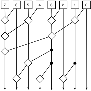
Just came across an interesting one, the Brent-Kung adder circuit, while looking at this TTL simulator in the browser

Image


Top
 Profile  
Reply with quote  
PostPosted: Wed Nov 04, 2020 11:36 am 
Offline
User avatar

Joined: Fri Nov 09, 2012 5:54 pm
Posts: 1431
Did a simulation in C.
Attachment:
BK_ADD.C [2.21 KiB]
Downloaded 69 times

Looks like implementing the Brent-Kung adder >carry chain topology< with FET SPDT pass_through switches won't be too efficient.
Ripple carry adder: carry chain has 8 SPDT switches. Brent-Kung adder: carry chain has 15 SPDT switches.

Also, with the Brent-Kung adder carry chain we would have a select_to_output delay of two switches for the MSB,
with 2.5V powered 74AUC2G53 switches this would be 2.8ns typ.

Attachment:
bk_adder_carry.png
bk_adder_carry.png [ 78.4 KiB | Viewed 1149 times ]

Haven't checked my wiring above for errors, because I'm not sure if implementing a Brent-Kung adder for our project would be a good idea.
Edit: Q0=P0, that text didn't make it into the schematic when cutting the screenshot to size.

// I love that smell of undigested scientific articles in the morning...


Top
 Profile  
Reply with quote  
PostPosted: Wed Nov 04, 2020 3:45 pm 
Offline
User avatar

Joined: Sun Oct 18, 2015 11:02 pm
Posts: 428
Location: Toronto, ON
Interesting concept BigEd and great work Dieter. The FET Switch has such asymmetrical behaviour and it’s a whole new dimension to consider. It seems a carry-select arrangement might work (compute the high-nibble with carry low and high in parallel). But even then, the tradeoff is the select time of the final switch vs. the added delay due to capacitance of the upper nibble in series.

_________________
C74-6502 Website: https://c74project.com


Top
 Profile  
Reply with quote  
PostPosted: Wed Nov 04, 2020 4:34 pm 
Offline
User avatar

Joined: Thu Apr 11, 2019 7:22 am
Posts: 40
Drass wrote:
The FET Switch has such asymmetrical behaviour and it’s a whole new dimension to consider
Or we could say it's an old dimension, because the relay computer engineers or the past designed their ALUs on the consideration of asymmetrical behaviour of mechanical relays :D


Top
 Profile  
Reply with quote  
PostPosted: Thu Nov 05, 2020 8:49 am 
Offline
User avatar

Joined: Fri Nov 09, 2012 5:54 pm
Posts: 1431
Joan, you happen to have some schematics at hand ?

The relay computer engineers probably didn't have to worry much about capacitances. :)

;---

Binary Adder Architectures for Cell-Based VLSI and their Synthesis, Reto Zimmerman 1997.
That's a nice read about adder topologies.

Tricks like in the picture below probably won't bring us far,
because ALU A inputs directly would be feeding the carry chain (piling up capacitances):
Attachment:
fulladder_a.png
fulladder_a.png [ 5.5 KiB | Viewed 1077 times ]

On PDF page 45, the conditional-sum adder structure looks interesting.

;---

High-Speed VLSI Arithmetic Units: Adders and Multipliers, Prof. Vojin G. Oklobdzija 1999
mentions on PDF page 15, that a conditional-sum adder was used at Byte level in the DEC "Alpha" 21064.

But implementing a conditional-sum adder at Bit level would be a lot of 74AUC2G53 switches (and a lot of capacitance).
While propagation delays of 4 Bit 2:1 multiplexers are slow, their switching time delays are not.

To me, conditional-sum adders don't look like the thing for our project. //Somebody please prove me wrong.


Top
 Profile  
Reply with quote  
PostPosted: Fri Nov 06, 2020 10:31 pm 
Offline
User avatar

Joined: Thu Apr 11, 2019 7:22 am
Posts: 40
Hi Dieter,

Quote:
Joan, you happen to have some schematics at hand ?

The relay computer engineers probably didn't have to worry much about capacitances. :)
The only public documentation that I am aware of, is from the Konrad Zuse Internet Archive. But last time I checked, the link was broken http://zuse.zib.de The Facom 128 from Japan is a more powerful one, still maintained and working at amazing specs. With its 68 bit bus, it performs floating point multiplication in 0.4 seconds max, and division or square root in 1.0 seconds. But I'm not aware of any public docs. The key for performance was a very wide bus (carry chains have zero delay), and an all parallel ALU. To help reliability, floating point numbers were represented on bi-quinary coded decimal and contacts were never switched with current. There's also a number of 'modern' relay computers made by hobbyists, but they are all based on modern CPU architectures, with virtually zero degree of parallelism and much narrower bus (maybe just 8 or 16 bits), resulting in much slower speeds than the original ones, despite using much faster relays. An interesting project would be to make a relay logic based computer with 74CBT3xxx analog switches.


Top
 Profile  
Reply with quote  
PostPosted: Sat Nov 07, 2020 3:20 am 
Offline
User avatar

Joined: Sun Oct 18, 2015 11:02 pm
Posts: 428
Location: Toronto, ON
The Facom 128 is amazing! Here is a nice video with a live demo of the machine. Thanks for pointing us to it Joan.

_________________
C74-6502 Website: https://c74project.com


Top
 Profile  
Reply with quote  
PostPosted: Sun Nov 08, 2020 1:06 am 
Offline
User avatar

Joined: Sun Oct 18, 2015 11:02 pm
Posts: 428
Location: Toronto, ON
Found this link about Konrad Zuse’s Z1 Computer: Architecture and Simulation of the Z1 Computer. It includes an interactive 3D simulation of the adder (pic below), and a informative pdf about the Z1 computer.
Attachment:
EEFB8A59-73A9-4CBB-B025-D2F5821E5370.jpeg
EEFB8A59-73A9-4CBB-B025-D2F5821E5370.jpeg [ 59.8 KiB | Viewed 983 times ]

_________________
C74-6502 Website: https://c74project.com


Top
 Profile  
Reply with quote  
Display posts from previous:  Sort by  
Post new topic Reply to topic  [ 182 posts ]  Go to page Previous  1 ... 3, 4, 5, 6, 7, 8, 9 ... 13  Next

All times are UTC


Who is online

Users browsing this forum: No registered users and 21 guests


You cannot post new topics in this forum
You cannot reply to topics in this forum
You cannot edit your posts in this forum
You cannot delete your posts in this forum
You cannot post attachments in this forum

Search for:
Jump to: