We're picking up where we left-off on Ideas for a faster TTL CPU. Team C74 is once again on hand and the objective is to build a next generation TTL 6502 with the highest clock-rate we can muster. The focus will be on reducing the cycle-time while keeping CPI fixed. The over-arching goal as always is to learn and to have fun. This project promises ample opportunity for both, so we'll buckle-up and get ready for a bumpy ride!
The effort breaks down into a few key strategies:
1) Use faster hardware
2) Optimize critical circuits
3) Increase parallel processing
4) Manage signal integrity
Let's look briefly at each in turn.
Memory is a key area where faster hardware is essential. Both external memory and the microcode store will need to keep up with a faster clock-rate. Fortunately, access-time can be reduced almost at will using RAM. Hobby-friendly 10ns RAMs are readily available, and synch RAMs are even faster. The latter expect an addresses in advance of the cycle, and deliver in return access-times that are vanishingly small. It's safe to say memory is not likely to be a bottleneck in this design.
By the same token, there are also faster logic families available. The 3.3V LVC family, for example, has a good selection of parts at almost twice the speed of AC logic. The CBTLV family offers 3.3V variants of FET switches which can be very fast when deployed correctly. And then there is the AVC and AUC families. With near-nanosecond propagation delays, these families also feature variable impedance outputs which "provide great signal integrity without the need for external termination when driving traces of moderate length (less than 15 cm)". All-in-all, it's an embarrassment of riches when it comes to fast components.
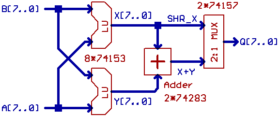
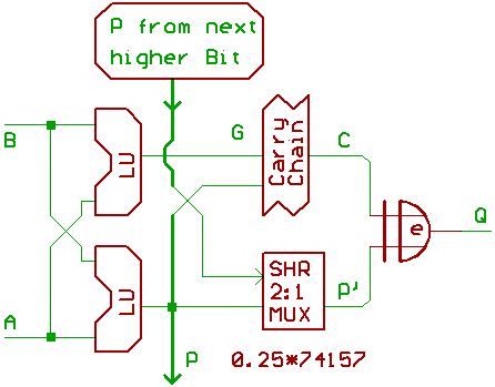
But there are limitations also. For example, there is no equivalent to the 74AC283 Adder in these faster families, and FET switches are no faster with Select signals than their AC family cousins. Some careful design will be needed in critical circuits to capture the potential gains. Dieter's FET Switch Adder is a good example this, but there are others. The Decode, Flag Evaluation, and Branch Testing circuits are a few examples that are likely to land on the critical path.
Beyond specific optimizations, we'll need to look to increased concurrency. The C74-6502 divided its processing into two stages: the FETCH stage, and the everything-else-stage (aka EXECUTE). An obvious improvement is to split EXECUTE into shorter phases. As we discovered, pipelining can get very complicated very quickly, with multiple caches, hazard checks and branch prediction schemes. So we'll need to be careful lest the whole thing get out of hand. Thankfully, there are significant gains to be had with more TTL-friendly techniques. More on that later.
The final leg of the race is all about signal integrity. Trace geometry, stackup and clock management will all need careful attention. We are likely to need six layers boards, impedance controlled traces and a mixed-voltage supply. It's gonna be fun. (My new bedtime reading is Dr. Johnson's Handbook Of Black Magic)
Alright, so that pretty much lays it out. It's good to be back with Team C74, and we're looking forward to the thrills and spills of this design. But let's take a moment now to pay homage to what is probably the fastest discrete component CPU ever built -- the Fluroinert-cooled Cray 2 supercomputer, clocking in with a 4.1ns cycle in 1985. It's a sight to behold:

I will never forget standing in a darkened observation gallery at Cray Research in the late eighties, and peering into the blueish glow of the demo-lab. Two lab-coated engineers were soberly pulling boards from that now famous circular tower at the center of the room. It was the stuff of legends. The Cray 2’s predecessor, the aptly-named Cray 1, had topped out at 85MHz in 1976, and here was a 244MHz machine. It was not until 1992 that DEC Alpha and HPPA RISC finally took the industry as whole beyond the 100MHz mark.
So is it possible for a discrete-component 6502 to reach that same 100MHz milestone? Well, we're gonna try to find out!
Cheers for now,
Drass
P.S. I wonder how hard Seymour would have worked to try to clip off that last 100ps from the 4.1ns critical path?
——————————-
Quick Links
For easy reference, here are some links to posts on specific topics:


