John West wrote:
One way to check would be to design a PCB for it. Lay the components out in the same positions as the original, and follow the original path for the tracks when you connect each net. If you end up with any unrouted nets, or tracks that the original board has but you don't, you'll know where your schematic was wrong. That's a lot of work, and needs clear pictures of both sides of the original board (including under the components). But if your aim is to recreate the PCB in modern tools, you'll be doing that work anyway.
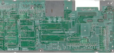
I have a PCB with no parts:
Attachment:
File comment: Commodore 16 PCB, top side
 C16-top.png [ 3.34 MiB | Viewed 1272 times ]
Unfortunately the board warped. I wonder if it was the hot air that warped the board or if (to some extent) the parts were keeping the 36 year old PCB flat. It's now on a cast iron machine table under a truck battery in an attempt to make it flat again. The silkscreen is slightly blurry in the top left corner. It's more noticeable on the original image (the attachment is 1/7th scale).
The board doesn't quite fit in my scanner. Can anyone recommend software to stitch multiple images together like the "panorama" photo mode on some phones?
For the traces, I had been hoping to lay out the parts on the PCB, skip the routing and post-process the scan of the board to a monochrome image showing copper and not-copper and then use the footprints and layout to automatically generate a net list based on which pins touch which other pins via the copper. Is there software out there for this sort of thing?


