6502.org Forum  Projects  Code  Documents  Tools  Forum
It is currently Sun Nov 10, 2024 10:55 pm

All times are UTC


Post new topic Reply to topic  [ 581 posts ]  Go to page Previous  1 ... 20, 21, 22, 23, 24, 25, 26 ... 39  Next
Author Message
PostPosted: Thu Feb 20, 2020 8:27 am 
Offline
User avatar

Joined: Thu May 28, 2009 9:46 pm
Posts: 8481
Location: Midwestern USA
floobydust wrote:
I also inspect them with a fairly powerful magnifier lens to ensure the solder joints are clean and without any bridging. I also have the same magnifier headset you picked up, but have not yet had a chance to use it for PCB work.

The magnifier headset I have isn't useful for soldering—the focal length is too short, but is invaluable for inspection. It's got a lot of magnification, and the pins on a DIP package look like railroad spikes through it. For assembly work, I use a five diopter lighted magnifier that I've had for many years. I wish I could find one with more magnification, but they don't seem to be available.

Quote:
I do wish you the best in working under the limited sight conditions you have... if you get into a bind, I'm happy to help out on soldering.

I appreciate the offer.

At this point in time, I'm unsure about how much longer I will be able to do this stuff. Even reading a computer screen is starting to be a challenge. I'm scheduled to be evaluated for participation in a clinical trial of a drug that might be able to partially reverse the vision problem. I was in a similar trial in 2016, but (literally) saw no improvement after six months of treatments and subsequently had worsening symptoms. So I'm not setting future goals too high.

First step is to get V1.2 to run. :D

_________________
x86?  We ain't got no x86.  We don't NEED no stinking x86!


Top
 Profile  
Reply with quote  
PostPosted: Thu Feb 20, 2020 3:42 pm 
Offline

Joined: Wed Feb 12, 2014 1:39 am
Posts: 173
Location: Sweden
That looks really good, I like that ZIF socket much better than the eject-a-dip

Had a look at the schematic, It looks like the Anode of your IRQ LED goes to GND instead of VCC?


Top
 Profile  
Reply with quote  
PostPosted: Thu Feb 20, 2020 4:05 pm 
Offline
User avatar

Joined: Thu May 28, 2009 9:46 pm
Posts: 8481
Location: Midwestern USA
LIV2 wrote:
That looks really good, I like that ZIF socket much better than the eject-a-dip.

It's somewhat more expensive that the Eject-A-DIP but easier to use. Also, it doesn't consume as much PCB space as the Eject-A-DIP. Note on the bare board picture the layout is for the Eject-A-DIP.

Quote:
Had a look at the schematic, It looks like the Anode of your IRQ LED goes to GND instead of VCC?

Oops! :oops: You're correct. Not only is that error on the schematic, it was carried over to the PCB. So it looks as though I will have to hack the unit even before powering it the first time. :twisted:

As I was saying above, vision isn't one of my strong suits. :(

_________________
x86?  We ain't got no x86.  We don't NEED no stinking x86!


Top
 Profile  
Reply with quote  
PostPosted: Fri Feb 21, 2020 1:27 am 
Offline

Joined: Wed Jan 08, 2014 3:31 pm
Posts: 578
I used the same ZIF socket on my home brew EEPROM programmer and 6502 SBC. They're definitely worth it and take both less space on the board and have a lower profile.


Top
 Profile  
Reply with quote  
PostPosted: Fri Feb 21, 2020 3:46 am 
Offline
User avatar

Joined: Thu May 28, 2009 9:46 pm
Posts: 8481
Location: Midwestern USA
BigDumbDinosaur wrote:
LIV2 wrote:
Had a look at the schematic, It looks like the Anode of your IRQ LED goes to GND instead of VCC?

Oops! :oops: You're correct. Not only is that error on the schematic, it was carried over to the PCB. So it looks as though I will have to hack the unit even before powering it the first time. :twisted:

As I was saying above, vision isn't one of my strong suits. :(

Okay, the plot thickens, so to speak. I applied power to the contraption and neither of the status LEDs illuminated. The "power good" green LED should have illuminated as soon as the board came out of reset. The "reset active" red LED should have illuminated while reset was in progress. Both are driven by the inverted reset signal, which the logic probe says is present. That is to say, the reset circuit is properly working.

Knowing that, a little digging confirmed my suspicions. The object I used to represent LEDs in the PCB layout has pins 1 and 2 reversed. Yep! Both LEDs are installed backwards! Adding insult to injury, I had created a new LED object a long time ago with the correct pin numbering, but forgot all about it and why I created it. Fortunately, extracting and replacing the two LEDs isn't too difficult. :twisted: :twisted: :twisted: That will get done at the same time I hack the IRQ LED so its anode is hooked up to Vcc, not ground.

:oops: :oops: :oops:

FYI to other users of the Express PCB software: the T 1-3/4 LED object is wrong.

_________________
x86?  We ain't got no x86.  We don't NEED no stinking x86!


Top
 Profile  
Reply with quote  
 Post subject: POC Computer Version One
PostPosted: Fri Feb 21, 2020 2:34 pm 
Offline

Joined: Thu Apr 19, 2018 12:53 pm
Posts: 25
Most likely you know.... I would suggest to test the LED's before you put them back.
Many LED's have a low reverse breakdown voltage.
An Ohm meter in the setting Diode will make the LED's light up. (faintly) Even if they're still in the circuit)


Top
 Profile  
Reply with quote  
PostPosted: Fri Feb 21, 2020 6:02 pm 
Offline

Joined: Mon May 21, 2018 8:09 pm
Posts: 1462
I think the reverse breakdown voltage of most through-hole LEDs is specified to be at least a little above 5V, so unlikely to have been damaged by a few minutes in that condition.


Top
 Profile  
Reply with quote  
PostPosted: Fri Feb 21, 2020 8:12 pm 
Offline
User avatar

Joined: Thu May 28, 2009 9:46 pm
Posts: 8481
Location: Midwestern USA
Guus Assmann wrote:
Most likely you know.... I would suggest to test the LED's before you put them back. Many LED's have a low reverse breakdown voltage. An Ohm meter in the setting Diode will make the LED's light up. (faintly) Even if they're still in the circuit)
Chromatix wrote:
I think the reverse breakdown voltage of most through-hole LEDs is specified to be at least a little above 5V, so unlikely to have been damaged by a few minutes in that condition.

Rather than take the chance that the LEDs were harmed by being reversed-biased, I will install new ones—I've got a lot of them. I'm hoping to get it done over the weekend.

_________________
x86?  We ain't got no x86.  We don't NEED no stinking x86!


Top
 Profile  
Reply with quote  
PostPosted: Sat Feb 22, 2020 12:43 am 
Offline
User avatar

Joined: Tue Mar 05, 2013 4:31 am
Posts: 1385
First, really nice job on soldering the PCB up... looks great, SMT and all. Second, ugh... bad LED layout, but that's an easy fix when installing a new one.

Interested to see your progress on the software side once you have the hardware sorted. I've also been using a ZIF socket on one of my SBC boards, which is used with a couple extra machined IC sockets to lift it above the board enough to clear other components. Here's the one I've been using for years:

https://www.mouser.com/ProductDetail/Ar ... oKddG8c%3D

Luckily, I've got 3 additional SBCs that have been running almost non-stop for 2+ years. I do dev work and test on the SBC with the ZIF socket, then do longer term testing on the other trio to ensure the code is stable.

_________________
Regards, KM
https://github.com/floobydust


Top
 Profile  
Reply with quote  
PostPosted: Sat Feb 22, 2020 1:14 am 
Offline
User avatar

Joined: Thu May 28, 2009 9:46 pm
Posts: 8481
Location: Midwestern USA
floobydust wrote:
First, really nice job on soldering the PCB up... looks great, SMT and all.

I can't take credit for all of it—the SMT stuff was done for me.

Quote:
I've also been using a ZIF socket on one of my SBC boards, which is used with a couple extra machined IC sockets to lift it above the board enough to clear other components. Here's the one I've been using for years:

I have that socket. It's somewhat on the bulky side, which is what led me to using the socket seen in the above photos.

_________________
x86?  We ain't got no x86.  We don't NEED no stinking x86!


Top
 Profile  
Reply with quote  
PostPosted: Wed Feb 26, 2020 8:21 am 
Offline
User avatar

Joined: Thu May 28, 2009 9:46 pm
Posts: 8481
Location: Midwestern USA
BigDumbDinosaur wrote:
First step is to get V1.2 to run. :D

After tripping over my shoelaces, metaphorically speaking, I've gotten V1.2 running.

The initial testing was with a "NOP generator," which is actually a ROM with a bunch of NOPs burned into it. The purpose was to exercise the 65C816 while watching for signs of spurious chip selects, inopportune writes, etc. In V1.2, ROM extends from $D000 to $FFFF (12KB), so the plan was to burn NOPs from $0000 in the ROM to $2FF8, followed by $4C $00 $D0, which is JMP $D000. Immediately after that is $00 $D0, which is the reset jump vector. Simple enough.

Upon inserting the ROM and powering up, I could see activity but also could see both the ROM and RAM being selected, as well as some write operations taking place. Worse yet, I/O chip selection was mixed in with the other activity. None of that was supposed to be happening. The code burned into the ROM was supposed to return the MPU to $D000 when it got to the top, without touching RAM or I/O. Clearly things weren't going as planned.

Just to be sure, I burned another ROM with the exact same content and read it back in the EPROM burner to verify a successful burn. A dodgy ROM wasn't the problem.

The next step was to revisit the glue logic and find the error that just had to be there. After carefully going through the logic step-by-step I was certain there were no errors.

That, in turn, led me to inspect the board under strong magnification to find the bad solder joint or solder bridge that was causing all the trouble. :shock: There was no bad solder joint or bridge causing trouble. Also, no chips were installed backwards. At that point, it wasn't looking like a hardware problem anymore.

So I decided to dust off an old gadget that anyone debugging 65xx hardware should have: a clock single-stepper. As V1.2 uses a flip-flop to condition the clock oscillator output, a dampened (debounced) push button can be used to toggle Ø2. WDC MPUs can be safely halted by stopping Ø2 in either phase, a feature that can be very helpful in troubleshooting that recalcitrant gadget you just built.

My original design used a Maxim DS1813 to dampen the push button. However, the clock would sometimes double-toggle, which I subsequently determined was due to the DS1813 generating an occasional runt pulse. So I decided to go a different route. Here's the circuit I used.

Attachment:
File comment: Clock Single-Stepper
pushbutton_damping.gif
pushbutton_damping.gif [ 5.49 KiB | Viewed 16178 times ]

Each push of the button will cause CLK to go high, causing the clock flop on V1.2 to toggle. Hence Ø2 will change state with each push of the button—two successive pushes constitute one Ø2 cycle. The R-C circuit attached to the input of the Schmitt trigger causes a relatively slow voltage rise after the push button has been pressed and released. The circuit's time-constant is sufficient to delay the Schmitt's change-of-state until well after contact bounce has ceased in the push button. I chose a time-constant of 100 milliseconds to avoid accidentally double-clocking.

Incidentally, a 74HC14 can be used here, as operating speed is obviously not critical. I used the 'AC14 because there was one in the junk pile.

Anyhow, after hooking up the above gadget and doing some probing and thinking it became clear why the unit was misbehaving. The ROM's /CS is asserted any time the address is $D000 to $FFFF. That translates to $1000-$3FFF in the ROM, due to decoding starting on an "odd" page ($DO). Where the shoelace tripping came in was when I burned the ROM image to $0000 instead of $1000 to compensate for the "odd" starting page. The MPU vector ($D000) was burned at $2FFC-$2FFD in the ROM, but when the MPU went to read a vector following reset it was reading from $3FFC and $3FFD. Nothing above $2FFF in the ROM had been altered, so the MPU was loading $FFFF as the reset vector. The result was the MPU went to $FFFF for its first instruction, where it found (you guessed it) $FF. :o

The opcode $FF is SBC <addrl>,X with the 65C816, <addrl> being a 24-bit address. As opcode and operand fetches cannot span banks, the operand for this bogus instruction was fetched from $0000-$0002 when PC wrapped. Once the MPU had finished subtracting garbage from garbage it loaded whatever was at $0003 as the next instruction, and off it went to who-knows-where. RAM is from $0000-$BFFF and I/O is at $C000. So as the MPU was merrily tiptoeing through the tulips, it was touching RAM and I/O, taking unknown branches, whacking the stack, engaging in wild writes, etc. This is because when first powered up, static RAM is filled with lots of random garbage.

Anyhow, I burned a fresh ROM with the code correctly positioned, inserted it and single-stepped to see if the correct vector would be gotten by the MPU. It was, so I reinstalled the clock oscillator and let it run while I probed various parts of the circuit to see how things were working.

It appears at this point V1.1 is functional. So the next step will be to test code that should write to the console screen. I will post pictures once that happens.

_________________
x86?  We ain't got no x86.  We don't NEED no stinking x86!


Top
 Profile  
Reply with quote  
PostPosted: Thu Feb 27, 2020 10:57 pm 
Offline
User avatar

Joined: Thu May 28, 2009 9:46 pm
Posts: 8481
Location: Midwestern USA
In my previous post, I mentioned how I used a clock single-stepper to figure out why POC V1.2 was stubborn about running. Here are some picture of the single-stepper. Be prepared to see a crude hack-job using odds and ends I had laying around in the shop.

Attachment:
File comment: Clock Single-Stepper Top View
single_stepper02.gif
single_stepper02.gif [ 1.52 MiB | Viewed 16131 times ]
Attachment:
File comment: Clock Single-Stepper Bottom View
single_stepper03.gif
single_stepper03.gif [ 1.5 MiB | Viewed 16131 times ]

Above are top and bottom views of the clock stepper, which will work in any circuit in which the oscillator drives a C-D flip-flop. I believe I have about $3.00 invested in this gadget. That's what I like: cheap test gear.

Attachment:
File comment: POC V1.2 w/Clock Stepper
single_stepper04.gif
single_stepper04.gif [ 1.17 MiB | Viewed 16131 times ]

Above is the stepper plugged into the clock oscillator socket on the board. Crude but effective. Also, note the hacked-up IRQ "heartbeat" LED to get it correctly situated in the circuit (bottom center of photo). In the schematic, I accidentally connected the LED's anode to ground instead of Vcc. That error, of course, got carried over to the PCB, but fortunately was spotted by an alert reader before I had gotten around to powering the unit and possibly having an electronic train wreck.

Speaking of the IRQ LED, I tinkered with one of the circuit values so the LED is dim when only the 100 Hz jiffy IRQ is present. When any significant IRQ activity occurs the LED brightens up quite a bit. If it goes out...

V1.2 is now fully functional, currently running on a 12.5 MHz clock with slightly modified V1.1 firmware. The only significant changes to the code were in the memory map assignments. Those are made in an INCLUDE file, so all that was necessary was to edit that one file, reassemble the code and burn a ROM from the object file. This points out the value of not embedding "magic numbers" such as addresses or constants directly in code, but instead externally defining them. If I had embedded the memory map assignments in code statements I'd still be picking through the source files looking for them and likely missing one or two in the process.

Anyhow, here is a screen shot of V1.2's POST display.

Attachment:
File comment: POC V1.2 Power-On, Self-Test (POST) Display
post_display.gif
post_display.gif [ 232.27 KiB | Viewed 16131 times ]

Next step will be to modify the serial I/O (SIO) primitives and interrupt handler (ISR) to recognize and drive the second DUART. The goal is to make both DUARTs look like a single QUART from a software point-of-view. I call this a vQUART (virtual QUART), since it's a software illusion.

The ISR actually is relatively simple to rework, since it already has the indexing features needed to address multiple SIO channels.¹ The SIO foreground is going to be a little more involved, since any SIO calls to the BIOS API have to be able to select the desired channel with as little hassle as possible. I'm thinking the best way to do this would be to load the X-register with the (zero-based) channel number and then call the BIOS function. For example, the code to send a datum out from channel C (the third channel) would be something like:

Code:
;   write datum to SIO channel C...
;
         lda #datum            ;what we're writing
         ldx #2                ;channel C's zero-based index
         pea #_sioout_         ;BIOS API index for SIO output
         cop #$00              ;call BIOS API function
         bcs error

All that mumbo-jumbo could be wrapped up in a tidy macro for C-programmers who only venture into assembly language when desperate: :D

Code:
;   write datum to SIO channel C using macro...
;
         sioout 'C','#',datum,error

This macro would convert 'C' at assembly-time to the proper channel index or halt assembly with an error if the index is out-of-range. The macro would then evaluate the second parameter to determine how to evaluate the datum parameter. '#' would tell the macro that datum is an immediate value, causing code generation equivalent to the previous example. If the second parameter is null, i.e., '' (two single quotes with nothing in between them), it would mean datum is an address at which the datum is to be found. Anything else would cause an assembly-time error.

If a fourth parameter is passed to the macro it will be understood to be an error vector (the error macro parameter). During macro expansion, code will be assembled to cause a branch to the vector if the API call returns an error. Otherwise, execution will continue in-line after the macro expansion.

Anyhow, that's the theory. Now to write the code that will make it work. :D

——————————
¹The channel indexing method I've been using in POC V1.1's firmware makes use of the (<dp>,X) addressing mode, as the channel pointers are arrayed on direct (zero) page. So all that is necessary, for example, to read from a particular channel is to load the channel index into .A, double it with an ASL instruction, copy it to .X and then execute LDA (<dp>,X), where <dp> is the base address of the channel receiver pointers. Who says (<dp>,X) addressing is useless? :shock:

_________________
x86?  We ain't got no x86.  We don't NEED no stinking x86!


Last edited by BigDumbDinosaur on Tue Mar 17, 2020 6:14 am, edited 1 time in total.

Top
 Profile  
Reply with quote  
PostPosted: Mon Mar 02, 2020 7:18 am 
Offline
User avatar

Joined: Thu May 28, 2009 9:46 pm
Posts: 8481
Location: Midwestern USA
As earlier stated, the purpose of POC V1.2 is to develop some hardware and programming concepts that can be applied to other hardware later on. Two hardware concepts embodied in V1.2 are the vQUART (virtual QUART) and interrupt "steering."

When I decided to implement the vQUART I realized I was going to have a lot of potential interrupt sources to service. Since there are four communications channels, there are four receivers and four transmitters that can interrupt—possibly all at the same time. Also, the DUARTs each have a timer that could generate an IRQ, which the timer in one of the DUARTs does at 10 millisecond intervals. Hence interrupt steering becomes important when a large number of IRQ sources exist in a system. Otherwise, significant MPU time may be consumed in figuring out which device is interrupting and why.

As the bulk of the IRQs that will be generated will be due to communications activities, I took advantage of a somewhat arcane DUART hardware feature to set up my interrupt steering. In a previous post, I wrote:

Quote:
Speaking of interrupts, the 28L92 can be configured so general purpose output pins 4, 5, 6 and 7 (OP4-7) act as open-drain IRQ signals. OP4 is wired to the RxD channel 1 IRQ, OP5 is wired to the RxD channel 2 IRQ, and OPs 6 and 7 are wired to the channel 1 and channel 2 transmitters, respectively. When the 28L92 interrupts with its main IRQ output, it will also pull one or more of these pins low if reception and/or transmission activity was the cause of the interrupt.

In order to take advantage of this feature, I have the OPs wired to the inputs of a 74ACT540 bus driver, with bits 0-3 wired to the receiver IRQs and bits 4-7 wired to transmitter IRQs—bits 0 and 4 are channel A, bits 1 and 5 are channel B, and so forth. The bus driver is assigned a location in the I/O map (designated SIOQ) which when read, will return a real-time IRQ status. If %00000000 is read, then no receive or transmit IRQs were generated. Otherwise, bits will be set according to what interrupted. These bits are real-time, meaning they stay set until the cause of the IRQ has been cleared.

This arrangement doesn't report the cause of other vQUART IRQs, such as timer underflow, which must be detected by reading the individual DUART interrupt status registers. However, the interrupt service handler's work will greatly reduced, since no polling of each receiver and transmitter will be required. This reduction becomes important when one considers that if all four channels are simultaneously receiving and transmitting at 115.2Kbps, as many as 46,080 IRQs due to SIO activity could occur in one second, assuming an IRQ occurs with each datum received or sent. In practice, the rate won't be quite as severe, due to the buffering provided by the DUARTs' FIFOs. In the best case, 2880 IRQs would occur each second of continuous bi-directional communication, as an interrupt will only come when a receiver FIFO is full or a transmitter FIFO is empty.

The basic circuit is pretty simple:
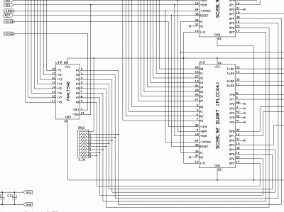
Attachment:
File comment: Serial I/O IRQ Steering Circuit
sio_irq_ckt.gif
sio_irq_ckt.gif [ 98.34 KiB | Viewed 16072 times ]

Below is a closeup of the hardware that implements this circuit.
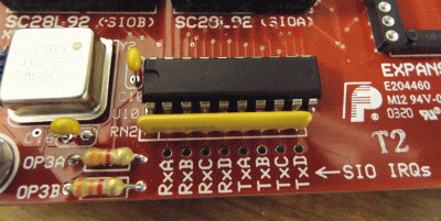
Attachment:
File comment: vQUART IRQ Steering Hardware
sio_irqs.gif
sio_irqs.gif [ 1.19 MiB | Viewed 16072 times ]

The 'ACT540 is wired so the individual bits read by the MPU are such that receiver IRQs are reported in the least significant nybble and the transmitter bits are reported in the most significant nybble. Bit 0 is channel A's receiver and bit 4 is channel A's transmitter. This arrangement makes it easy to process active IRQs in a succinct loop. Here's the code for processing receiver activity:

Code:
iirq0200 lda io_sioq           ;get vQUART channel IRQ status
         beq iirq0400          ;nothing to process
;
         bit #m_irqrx          ;receiver IRQ?
         beq iirq0310          ;no
;
         sta tiairqst          ;save IRQ status
         ldy #0                ;starting channel index
;
;
;   channel processing loop...
;
.0000010 lsr tiairqst          ;channel receiver interrupting?
         bcc .0000030          ;no, skip it
;
         tya                   ;yes, copy channel index &...
         asl A                 ;make channel pointer...
         tax                   ;offset
         lda #nxpcresr         ;clear any...
         sta (tiacr,x)         ;RxD overrun error
;
;
;   RHR processing loop...
;
.0000020 lda (tiasr,x)         ;get channel status
         bit #nxprxdr          ;RHR empty?
         beq .0000030          ;yes, done with channel
;
         lda (tiafif,x)        ;get & hold datum from...
         xba                   ;RHR
         lda tiaputrx,x        ;get queue 'put' pointer
         inc A
         cmp tiagetrx,x        ;any room in queue?
         beq .0000020          ;no, discard datum
;
         xba                   ;store datum...
         sta (tiaputrx,x)      ;in queue
         xba                   ;new 'put' pointer
         sta tiaputrx,x        ;store it &...
         bra .0000020          ;loop
;
;   ...end of RHR processing loop
;
;
.0000030 iny                   ;next channel
         cpy #n_nxpchn         ;all channels processed?
         bcc .0000010          ;no
;
;   ...end of channel processing loop

As can be seen, the body of this routine is an inner and outer loop. Prior to entering the loops, the value read from the interrupt steering hardware is tested to see if any receiver bits are set. If none is set the receiver processing code is completely skipped—there's nothing to process. :D

Upon determining at least one receiver has interrupted, the outer loop will start by right-shifting the value read from the interrupt steering hardware to determine which receivers require service. If the bit corresponding to any given receiver is cleared, the inner processing loop is skipped. Otherwise, the inner loop will repeatedly read the receiver holding register (RHR, aka FIFO) until the receiver status shows all datums have been gotten. If the circular queue into which the datums are to be stored is full the datum will be discarded. Once all datums have been gotten the IRQ for that receiver will be automatically cleared.

The code for processing transmitter IRQs is somewhat similar:

Code:
;vQUART TRANSMITTER IRQ PROCESSING
;
iirq0300 lda io_sioq           ;IRQ status
;
iirq0310 bit #m_irqtx          ;transmitter IRQ?
         beq iirq0400          ;no, done with vQUART
;
         sta tiairqst          ;save IRQ status
         ldy #n_nxpchn-1       ;starting channel
;
;
;   channel processing loop...
;
.0000010 asl tiairqst          ;transmitter interrupting?
         bcc .0000040          ;no, skip it
;
         tya                   ;copy channel index &...
         asl A                 ;make channel pointer...
         tax                   ;offset
;
;
;   THR processing loop...
;
.0000020 lda tiagettx,x        ;queue 'get' pointer
         cmp tiaputtx,x        ;queue 'put' pointer
         beq .0000030          ;nothing to transmit
;
         lda (tiasr,x)         ;get channel status
         bit #nxptxdr          ;THR full?
         beq .0000040          ;yes, done for now
;
         lda (tiagettx,x)      ;read queue &...
         sta (tiafif,x)        ;write to THR
         inc tiagettx,x        ;bump 'get' pointer &...
         bra .0000020          ;loop
;
;   ...end of THR processing loop
;
.0000030 lda #nxpcrtxd         ;disable...
         sta (tiacr,x)         ;TxD
         lda tiatstab,x        ;tell foreground...
         tsb tiatxst           ;about it
;
.0000040 dey                   ;all channels serviced?
         bpl .0000010          ;no
;
;   ...end of channel processing loop

Here again, the always-handy BIT instruction is used to determine if any transmitters are active—the entire code segment will be skipped if none is interrupting. However, for programming convenience, the outer loop works backwards through the channels as it services interrupting transmitters. The inner loop attempts to stuff as many datums into the transmitter's FIFO as possible, a procedure that assists in reducing IRQ servicing overhead.

During inner loop processing, there are three conditions that have to be accounted for:

  1. FIFO is full. If the FIFO is full, the inner loop is broken and further processing on the channel is deferred. The transmitter will not interrupt again until it has emptied its FIFO.

  2. There isn't enough data to fill the FIFO. If this happens the transmitter will be told to shut down after it has sent the final datum.

  3. There is no data to transmit. The transmitter will be immediately shut down.

Killing the transmitter when the data runs out is necessary to prevent it from continuously interrupting the MPU and causing deadlock. Due to the design of NXP UARTs, the transmitter can be told to shut down as soon as the data runs out, even if there are still datums in the FIFO waiting to be sent (and this can happen quite often with a serial hookup that uses hardware handshaking). The transmitter will continue to shift datums out on to the wire until the FIFO has emptied, at which time it will shut down. Shutting down the transmitter automatically disables the transmit IRQ. Note how a flag is set in the code to tell the foreground that the transmitter is dead and must be restarted when more data becomes available for transmission.

As can be seen, I've made extensive use of that useless (<dp>,X) addressing mode in implementing this driver. 8) During reset, an array of pointers is copied from ROM to direct page, three sets of pointers for each channel's chip registers. The expense of calculating or looking up the register addresses each time an interrupt is serviced is avoided. Also, there is an array of pointers for the circular queues associated with each channel. Again, this eliminates the need to do table look-ups or pointer arithmetic on each interrupt.

Here is a snippet from the list file for that part of the assembled code:

Code:
02980  ;   TIA-232 driver workspace...
02981  ;
02982    000E          tiazpptr =tdsecct+s_tdcnt      ;start of pointer array
02983    000E          tiasr    =tiazpptr             ;vQUART channel status
02984    0016          tiacr    =tiasr+s_nxpchp       ;vQUART channel command
02985    001E          tiafif   =tiacr+s_nxpchp       ;vQUART channel FIFO
02986    0026          tiagetrx =tiafif+s_nxpchp      ;RxD queue 'get'
02987    002E          tiaputrx =tiagetrx+s_nxpchp    ;RxD queue 'put'
02988    0036          tiagettx =tiaputrx+s_nxpchp    ;TxD queue 'get'
02989    003E          tiaputtx =tiagettx+s_nxpchp    ;TxD queue 'put'
02990    0046          tiatxst  =tiaputtx+s_nxpchp    ;TxD status (bit field)
02991    0047          tiairqst =tiatxst+s_byte       ;vQUART IRQ status workspace
02992  ;
02993    0048          zeropage .= tiairqst+s_byte    ;*** BIOS/kernel direct page end ***

Needless to say, if anything steps on that part of direct page there is going to be a computing train wreck. Incidentally, the TxD status bit field (tiatxst) is used to keep track of which transmitters have been shut down—a bit is set if the corresponding transmitter is down. The handy TRB and TSB instructions are used to manipulate this field.

Earlier this evening, I implemented the above code and much to my amazement, it worked on the first try. So that's one item that can be checked off the to-do list. :D

_________________
x86?  We ain't got no x86.  We don't NEED no stinking x86!


Top
 Profile  
Reply with quote  
PostPosted: Tue Mar 24, 2020 9:21 am 
Offline
User avatar

Joined: Thu May 28, 2009 9:46 pm
Posts: 8481
Location: Midwestern USA
POC V1.2 has been running continuously at 12.5 MHz since March 3 without a hitch. An attempt to run it at 14 MHz was unsuccessful. As all glue logic is 74AC, much of it with sub-10ns prop time, I suspect that the EPROM I have in the unit can't tolerate the resulting 70ns machine cycle. At some point, I may use one of my 45ns OTP ROMs to see if that is the case, although even that part may have trouble.

Otherwise, the unit is working fine and thanks to the downtime caused by COVID-19 and my strong desire to continue breathing, I am deep into redoing the firmware to convert from a jump table API to an API accessed using the COP software interrupt. The new firmware will also support all four serial channels, as well as have some new functions that will be useful when I do something boneheaded with software and semi-crash the machine. :D

Also close to being built will be a clock stretcher on a plug-in module. This thing will be rigged up so it holds Ø2 high for two additional cycles when ROM is accessed and for one additional cycle when I/O is accessed. The two-cycle ROM wait state should make it possible to use 70ns ROMs, which would otherwise be too slow to work reliably above 8 MHz. I hope to soon test out this thing.

_________________
x86?  We ain't got no x86.  We don't NEED no stinking x86!


Top
 Profile  
Reply with quote  
PostPosted: Tue Mar 24, 2020 7:30 pm 
Offline
User avatar

Joined: Thu May 28, 2009 9:46 pm
Posts: 8481
Location: Midwestern USA
Earlier, I wrote:

BigDumbDinosaur wrote:
Next step will be to modify the serial I/O (SIO) primitives and interrupt handler (ISR) to recognize and drive the second DUART...The SIO foreground is going to be a little more involved, since any SIO calls to the BIOS API have to be able to select the desired channel with as little hassle as possible. I'm thinking the best way to do this would be to load the X-register with the (zero-based) channel number and then call the BIOS function.

Having slept on this for a while, I decided that using .X to tell the SIO driver which channel to access is not the ideal route. Too much of my code uses .X in conjunction with repetitive SIO accesses, and as having to preserve the register and then load it with the desired channel for each SIO access call would be a hassle, I determined another method was needed. I considered pushing the channel before calling the SIO function, but deemed that too expensive in execution time due to the monkey-motion that would be required to fetch the channel and then clean up the stack.

Finally, I decided the way to do it is to have API functions to set the default input and output channels prior to SIO access. For example, it would be possible to direct all output to channel D and get all input from channel B without having to explicitly state the target channel with each access. Three API functions handle it:

Code:
;set channel D as default output...
;
        ldx #nxpchand         ;channel D
        cop kchout            ;set it as output
        bcs error             ;invalid channel

and

Code:
;set channel B as default input...
;
        ldx #nxpchanb         ;channel B
        cop kchin             ;set it as input
        bcs error             ;invalid channel

For convenience, a third call sets both defaults:

Code:
;set default input & output...
;
        ldx nxpchanb          ;B is default input channel
        ldy mxpchand          ;D is default output channel
        cop kchset            ;set both channels
        bcs error             ;invalid channel(s)

The above sets both channels. The function's code is written so that nothing is changed if one of the channels is invalid. A companion function gets the default channels and returns them to the caller.

With the default input channel set, a call to get a datum would be:

Code:
;read datum from default input...
;
        cop kchget            ;get a datum into .A
        bcs nodata            ;nothing to get — .A unchanged
;
        sta datum             ;datum returned in .A


Similarly, a call to output a datum would be:

Code:
;write a datum on default output...
;
        lda datum             ;datum to write
        cop kchput            ;write it

Internally, the SIO driver will use the default channel values previously set up (which are stored in one byte) to generate an index into the direct page pointer set that points to the circular queues associated with the target channels. The defaults stay unchanged until another call is made to kchin, kchout and/or kchset.

There are also API calls that directly access the console for input and output without getting the above mechanism involved. So I have the capability of a "standard input" and "standard output," as well as a "standard error." Obviously, this is not the same arrangement as found in UNIX, but is similar in spirit.

_________________
x86?  We ain't got no x86.  We don't NEED no stinking x86!


Top
 Profile  
Reply with quote  
Display posts from previous:  Sort by  
Post new topic Reply to topic  [ 581 posts ]  Go to page Previous  1 ... 20, 21, 22, 23, 24, 25, 26 ... 39  Next

All times are UTC


Who is online

Users browsing this forum: No registered users and 4 guests


You cannot post new topics in this forum
You cannot reply to topics in this forum
You cannot edit your posts in this forum
You cannot delete your posts in this forum
You cannot post attachments in this forum

Search for:
Jump to: