6502.org Forum  Projects  Code  Documents  Tools  Forum
It is currently Sat Nov 23, 2024 1:31 am

All times are UTC


Post new topic Reply to topic  [ 298 posts ]  Go to page Previous  1, 2, 3, 4, 5 ... 20  Next
Author Message
PostPosted: Fri Jan 24, 2020 8:36 pm 
Offline
User avatar

Joined: Wed Feb 14, 2018 2:33 pm
Posts: 1488
Location: Scotland
Proxy wrote:
I'd like to keep the system pure without an external device taking over (for now), i just asked because in WinCUPL a D-Flip Flop has 2 pins it likes you to connect to something to. "AR" (Async. Reset) and "SP" (Sync. Preset). if i leave them unconnected it doesn't spit out an error, just 2 warnings. i'll just leave them unconnected for now.


I wasn't suggesting you use another device - I just made the comment in-case you were wondering.

WinCUPL is more sophisticated than GALasm - you can do all that in GALasm, but it takes more lines of writing the terms out long-hand.

Quote:
what do you mean with a "TIL programmer"? I got the "TL866 II Plus" Programmer which worked perfectly fine last time i tested it.
Programming the GALs is pretty easy as well, i just do a "device specific compile" in WinCUPL, load the Generated .JED file into the Programmer's Software, and Program the chip.


I meant your TL866 programmer. Glad to hear it's programming them OK. Mine is the older one and it wouldn't although it advertised that capability )-: Are you using recycled Lattice ones of the current Microchip (Atmel) ones?

Cheers,

-Gordon

_________________
--
Gordon Henderson.
See my Ruby 6502 and 65816 SBC projects here: https://projects.drogon.net/ruby/


Top
 Profile  
Reply with quote  
PostPosted: Sat Jan 25, 2020 6:09 am 
Offline
User avatar

Joined: Fri Aug 03, 2018 8:52 am
Posts: 746
Location: Germany
drogon wrote:
I wasn't suggesting you use another device - I just made the comment in-case you were wondering.

WinCUPL is more sophisticated than GALasm - you can do all that in GALasm, but it takes more lines of writing the terms out long-hand.

Oh i see.

drogon wrote:
I meant your TL866 programmer. Glad to hear it's programming them OK. Mine is the older one and it wouldn't although it advertised that capability )-: Are you using recycled Lattice ones of the current Microchip (Atmel) ones?


I got the Lattice ones. i got like 15 of them for 15 bucks on Ebay. so far they have all been working.

but i think i should start with the most difficult part of the project... actually designing the PCB. and i have no idea how to actually do that.
i just know that you can generate a PCB from a schematic. so i'll try that. but i have to add some custom components and don't fully know everything that goes on the board yet.
so i feel like i'm missing a step


Top
 Profile  
Reply with quote  
PostPosted: Sat Jan 25, 2020 6:39 am 
Offline
User avatar

Joined: Wed Feb 14, 2018 2:33 pm
Posts: 1488
Location: Scotland
Proxy wrote:
drogon wrote:
I meant your TL866 programmer. Glad to hear it's programming them OK. Mine is the older one and it wouldn't although it advertised that capability )-: Are you using recycled Lattice ones of the current Microchip (Atmel) ones?


I got the Lattice ones. i got like 15 of them for 15 bucks on Ebay. so far they have all been working.


That's what I do too - so-far, so-good. It looks like they're board pulls, so +1 for recycling and hopefully they'll only have been programmed once for a production board.


Proxy wrote:
but i think i should start with the most difficult part of the project... actually designing the PCB. and i have no idea how to actually do that.
i just know that you can generate a PCB from a schematic. so i'll try that. but i have to add some custom components and don't fully know everything that goes on the board yet.
so i feel like i'm missing a step


I'd suggest, that if you have the time, that you get KiCAD installed and work through some online/youtube tutorials. This is where I want to get to, but having used Fritzing for the past 8 years, that's what I stick to for now. Fritzing has potential to be much much better, but it's development has paused and it's more or less a dead-end project right now.

The alternatives might be to use some of the online (web based) ones - I've no idea about these though. Eagle used to be the "go to" for small hobby projects too, but I think they've reduced the free support to something that's almost unusable now.

-Gordon

_________________
--
Gordon Henderson.
See my Ruby 6502 and 65816 SBC projects here: https://projects.drogon.net/ruby/


Top
 Profile  
Reply with quote  
PostPosted: Sat Jan 25, 2020 7:14 am 
Offline
User avatar

Joined: Fri Aug 03, 2018 8:52 am
Posts: 746
Location: Germany
drogon wrote:

I'd suggest, that if you have the time, that you get KiCAD installed and work through some online/youtube tutorials. This is where I want to get to, but having used Fritzing for the past 8 years, that's what I stick to for now. Fritzing has potential to be much much better, but it's development has paused and it's more or less a dead-end project right now.

The alternatives might be to use some of the online (web based) ones - I've no idea about these though. Eagle used to be the "go to" for small hobby projects too, but I think they've reduced the free support to something that's almost unusable now.

-Gordon


i already have KiCad and already tried myself at PCB design with it. for my old Z80 Computer... but as you might've guessed it ended up nowhere.
Though i know how to somewhat create custom symbols I will still look into some tutorials as that's basically where my knowledge ends.

i also need to look into what to do with all the pins of the 65C02 like the BE, VP, SYNC, etc.
i assume all outputs i don't need i just leave open, and all inputs i don't need i can just pull up/down through a resistor. (unless the CPU has internal pull-up/down resistors)


Top
 Profile  
Reply with quote  
PostPosted: Sat Jan 25, 2020 8:47 am 
Offline
User avatar

Joined: Wed Feb 14, 2018 2:33 pm
Posts: 1488
Location: Scotland
Proxy wrote:
drogon wrote:

I'd suggest, that if you have the time, that you get KiCAD installed and work through some online/youtube tutorials. This is where I want to get to, but having used Fritzing for the past 8 years, that's what I stick to for now. Fritzing has potential to be much much better, but it's development has paused and it's more or less a dead-end project right now.

The alternatives might be to use some of the online (web based) ones - I've no idea about these though. Eagle used to be the "go to" for small hobby projects too, but I think they've reduced the free support to something that's almost unusable now.

-Gordon


i already have KiCad and already tried myself at PCB design with it. for my old Z80 Computer... but as you might've guessed it ended up nowhere.
Though i know how to somewhat create custom symbols I will still look into some tutorials as that's basically where my knowledge ends.

i also need to look into what to do with all the pins of the 65C02 like the BE, VP, SYNC, etc.
i assume all outputs i don't need i just leave open, and all inputs i don't need i can just pull up/down through a resistor. (unless the CPU has internal pull-up/down resistors)


I did Ruby 6502 & 816 boards in Fritzing - this what the 816 one looks like: https://unicorn.drogon.net/ruby816-2.jpg

You need to keep BE, Rdy, /SO, /IRQ and /NMI pulled up, (3.3K is typical) however it may depend on the logic you use to drive them. Sync is output. Rdy is input and output, but unless you're using it then use a pull-up.

-Gordon

_________________
--
Gordon Henderson.
See my Ruby 6502 and 65816 SBC projects here: https://projects.drogon.net/ruby/


Top
 Profile  
Reply with quote  
PostPosted: Sat Jan 25, 2020 8:56 am 
Offline
User avatar

Joined: Fri Aug 03, 2018 8:52 am
Posts: 746
Location: Germany
drogon wrote:

I did Ruby 6502 & 816 boards in Fritzing - this what the 816 one looks like: https://unicorn.drogon.net/ruby816-2.jpg

You need to keep BE, Rdy, /SO, /IRQ and /NMI pulled up, (3.3K is typical) however it may depend on the logic you use to drive them. Sync is output. Rdy is input and output, but unless you're using it then use a pull-up.

-Gordon


That's a fine looking board. hoping that one day i have something similar in my hands.
and yea i used some picture online to see all the input pins that i don't need and just pull them up with a single resistor array (since i have a lot of those). though i'm using 4.7k resistsors since for some reason i have a lot more of those than 3.3k. but that shouldn't cause any issues.
and i also found out that i can download symbols/footprints for parts from Digikey and Mouser (not for all but most). so i don't even need to make a lot of the parts myself.
also i needed to redo the decoding a bit, again. because i forgot that i have 2 32kB RAM chips. so i need 2 CS lines for them. one for when RAM below 32k is accessed and one for when it's above. but that was a simple fix.

lastly, the RDY pin on the 65C02 is bidirectional so i cannot just hook it up straight to the GAL, i need a resistor in series with the pin. what's a good value for that? i currectly set it to be 4.7k. and does the RDY pin still need a pull-up when it's being held high by the GAL by default?


Top
 Profile  
Reply with quote  
PostPosted: Sat Jan 25, 2020 9:21 am 
Offline
User avatar

Joined: Fri Aug 30, 2002 1:09 am
Posts: 8544
Location: Southern California
Proxy wrote:
lastly, the RDY pin on the 65C02 is bidirectional so i cannot just hook it up straight to the GAL, i need a resistor in series with the pin. what's a good value for that? i currectly set it to be 4.7k. and does the RDY pin still need a pull-up when it's being held high by the GAL by default?

The 4.7K is probably fine but I would put a 22pF across the resistor to get rid of the RxC time constant of charging the parasitic capacitance on one side or the other.

_________________
http://WilsonMinesCo.com/ lots of 6502 resources
The "second front page" is http://wilsonminesco.com/links.html .
What's an additional VIA among friends, anyhow?


Top
 Profile  
Reply with quote  
PostPosted: Sat Jan 25, 2020 9:39 am 
Offline
User avatar

Joined: Fri Aug 03, 2018 8:52 am
Posts: 746
Location: Germany
GARTHWILSON wrote:
Proxy wrote:
lastly, the RDY pin on the 65C02 is bidirectional so i cannot just hook it up straight to the GAL, i need a resistor in series with the pin. what's a good value for that? i currectly set it to be 4.7k. and does the RDY pin still need a pull-up when it's being held high by the GAL by default?

The 4.7K is probably fine but I would put a 22pF across the resistor to get rid of the RxC time constant of charging the parasitic capacitance on one side or the other.

i assume a ceramic one because i don't think electrolytic ones can even go that low.

once i got a somewhat complete schematic i'll post it on here, then we can sort out any visible problems


Top
 Profile  
Reply with quote  
PostPosted: Sat Jan 25, 2020 10:01 am 
Offline

Joined: Mon May 21, 2018 8:09 pm
Posts: 1462
Also it has to be bipolar, which is more important, and electrolytics usually aren't bipolar.


Top
 Profile  
Reply with quote  
PostPosted: Sat Jan 25, 2020 10:23 am 
Offline
User avatar

Joined: Fri Aug 30, 2002 1:09 am
Posts: 8544
Location: Southern California
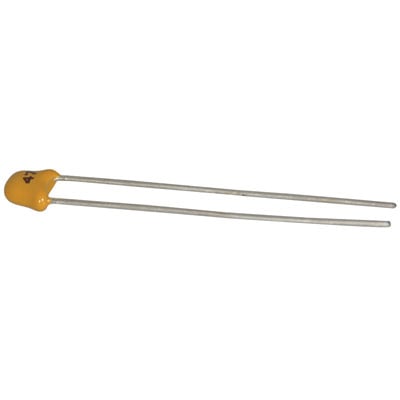
Yes, ceramic. It will probably look something like this:
Image
unless you do surface-mount and get a chip capacitor. The picture shows it several times actual size on my monitor.

_________________
http://WilsonMinesCo.com/ lots of 6502 resources
The "second front page" is http://wilsonminesco.com/links.html .
What's an additional VIA among friends, anyhow?


Top
 Profile  
Reply with quote  
PostPosted: Sat Jan 25, 2020 10:36 am 
Offline
User avatar

Joined: Fri Aug 03, 2018 8:52 am
Posts: 746
Location: Germany
Chromatix wrote:
Also it has to be bipolar, which is more important, and electrolytics usually aren't bipolar.

i thought all ceramic capacitors are bipolar so i didn't mention it

GARTHWILSON wrote:
Yes, ceramic. It will probably look something like this:
Image
unless you do surface-mount and get a chip capacitor. The picture shows it several times actual size on my monitor.

yep i got 3 boxes full of those, from 10pF to 10uF. so i probably won't need to order new ones any time soon

and i'd like to keep thing TH instead of SMD as i'm not experienced in soldering SMD stuff.
the exception on this board being the FT240X.


Top
 Profile  
Reply with quote  
PostPosted: Sat Jan 25, 2020 2:28 pm 
Offline
User avatar

Joined: Fri Aug 03, 2018 8:52 am
Posts: 746
Location: Germany
Ok, this is what i currently got for the Schematic.
there are barely any wires because i used Net's for basically everything.
PIC (posting as a Link because of the image's size. gotta love 4k Monitors)
it should have everything on it but i'm sure i missed something.
U0 -> 65C02 CPU
U1/2 -> GAL22V10 (i used a ATF22V10 for the symbol/footprint but they are pin compatible so it shouldn't matter)
U3 -> SN74HC541 Tri-State Buffer (used as the "STATUS" IO Device which allows the CPU to check if any data came in through USB and if data can be send)
U4 -> FT240X USB Interface
U5 -> 512kB FLASH Chip (8kB used, rest of Address lines are directly connected to GND)
U6/7 -> 32kB SRAM Chips
S0 -> Push button for Reset
J0 -> USB-B Connector (i like USB-B, it's TH instead of SMD like some Micro-USB connectors and is very durable)
J1 -> 32pin Pin Header (connects to a lot of important CPU Pins, can be used to hook up anything to the Computer, maybe i'll add more pins to allow RAM/ROM to be turned off so that additional Memory/ROMs can be added)
X0 -> 10MHz Clock Oscillator (i just choose a random one that had "14pin DIP" in the description)
RN0 -> 9pin Resistor Array (not sure if this is a good idea compared to regular resistors, one the one hand it'S more compact and easier to solder, on the other it would mean the PCB would need to route all of those connections to a single location instead of the Resistor being close to where it's needed)
R0 -> 4.7kΩ
R1/2 -> 27Ω (the FT240X datasheet had these resistors between the USB connector and the Chip)
C0 -> 22pF
C1/2 -> 47pF (same as with R1/2, the datasheet had 2 bipolar capacitors to ground for the data wires)
C3 -> 100uF (saw online that there should be an Electrolytic Capacitor close to the power input, in this case the USB Connector)
C4 -> Debounce capacitor for the Reset button
C5-12 -> 0.1uF (bypass capacitors for each IC, on the actual PCB they will be placed closer to each IC)

Hope this helps to explain the design and makes it easier to find mistakes and similar.

also note that with the exception of U6/7 (the RAM) all symbols were either included in KiCad or downloaded from Mouser

Top
 Profile  
Reply with quote  
PostPosted: Sat Jan 25, 2020 8:12 pm 
Offline
User avatar

Joined: Fri Aug 30, 2002 1:09 am
Posts: 8544
Location: Southern California
Quote:
C4 -> Debounce capacitor for the Reset button

I would not put a capacitor there. Some manufacturers made the RST\ input a Schmitt-trigger input, but WDC doesn't say anything about it, so it would take some experimentation to verify. I've run into a problem with that before with a different manufacturer. Generally you'll want that signal to come up all at once, debounced but with a fast rise time. It will take an active reset circuit to do this. See the Reset section of the 6502 primer at http://wilsonminesco.com/6502primer/RSTreqs.html . In fact, you would do well to read the entire 6502 primer, indexed at http://wilsonminesco.com/6502primer/ . There's so much there that will save you a lot of grief in the long run.

_________________
http://WilsonMinesCo.com/ lots of 6502 resources
The "second front page" is http://wilsonminesco.com/links.html .
What's an additional VIA among friends, anyhow?


Top
 Profile  
Reply with quote  
PostPosted: Sat Jan 25, 2020 8:47 pm 
Offline
User avatar

Joined: Fri Aug 03, 2018 8:52 am
Posts: 746
Location: Germany
GARTHWILSON wrote:
Quote:
C4 -> Debounce capacitor for the Reset button

I would not put a capacitor there. Some manufacturers made the RST\ input a Schmitt-trigger input, but WDC doesn't say anything about it, so it would take some experimentation to verify. I've run into a problem with that before with a different manufacturer. Generally you'll want that signal to come up all at once, debounced but with a fast rise time. It will take an active reset circuit to do this. See the Reset section of the 6502 primer at http://wilsonminesco.com/6502primer/RSTreqs.html . In fact, you would do well to read the entire 6502 primer, indexed at http://wilsonminesco.com/6502primer/ . There's so much there that will save you a lot of grief in the long run.


i looked through the primer a few times for stuff like decoding, interrupts, etc
but clearly didn't remember a lot.

so basically i should make the button active-high with a debouce capacitor and then invert the signal before sending it to the RST pin?
and is it nessesary to be a Schmitt trigger Inverter? if not i can just use 2 extra pins on my GALs to do the job.

speaking of which i also need a power-up reset circuit, so the CPU doesn't start execusing random garabge from RAM before reaching the ROM.
so that'll probably require another IC.


Top
 Profile  
Reply with quote  
PostPosted: Sat Jan 25, 2020 9:22 pm 
Offline
User avatar

Joined: Fri Aug 30, 2002 1:09 am
Posts: 8544
Location: Southern California
Proxy wrote:
so basically i should make the button active-high with a debouce capacitor and then invert the signal before sending it to the RST pin?
and is it nessesary to be a Schmitt trigger Inverter? if not i can just use 2 extra pins on my GALs to do the job.

The Schmitt trigger input is the whole reason for using that gate (an inverter in this case). A standard gate won't have the desired behavior. Its purpose is to take a slowly rising or falling voltage (like what's on a capacitor that's charging or discharging), and ignore noise on the line and suddenly flip the output when it reaches the right threshold. The threshold for going the other direction will be different. If you don't have any Schmitt-trigger gates in your personal stock and don't want to order and wait for one to arrive, you can make one by adding positive feedback with resistors. I show this kind of think in the last diagram at the bottom of http://6502.org/users/garth/projects.php?project=7, but you won't need the open-collector transistor at the output like I needed there to work with the other RST\ sources in the C64. That transistor inverts the signal again; so the rest of your circuit before that would be done in the opposite polarity.

Quote:
speaking of which i also need a power-up reset circuit, so the CPU doesn't start execusing random garabge from RAM before reaching the ROM.
so that'll probably require another IC.

No; if I understand you correctly, you're talking about the same circuit. After the power is up and stable, and the oscillator is stabilized, the reset circuit brings the RST\ line up with a single, fast rising edge, and the processor reads address $FFFC and $FFFD to get the address of where your reset routine in your ROM starts.

_________________
http://WilsonMinesCo.com/ lots of 6502 resources
The "second front page" is http://wilsonminesco.com/links.html .
What's an additional VIA among friends, anyhow?


Top
 Profile  
Reply with quote  
Display posts from previous:  Sort by  
Post new topic Reply to topic  [ 298 posts ]  Go to page Previous  1, 2, 3, 4, 5 ... 20  Next

All times are UTC


Who is online

Users browsing this forum: No registered users and 13 guests


You cannot post new topics in this forum
You cannot reply to topics in this forum
You cannot edit your posts in this forum
You cannot delete your posts in this forum
You cannot post attachments in this forum

Search for:
Jump to: