
I have been fixing some errors but there is still a long way to go I'm afraid. It takes the simulation up to 10 minutes to reach the point of interest, and looking at the log has its limits. Is there a way to split the test into smaller pieces, or to begin execution at a later time? I mean, has anyone done it before? Or any recommendations in order to do this myself. It would make debugging easier.
Juan
Micro programmed 6502-like CPU
-
DerTrueForce
- Posts: 483
- Joined: 04 Jun 2016
- Location: Australia
Re: Micro programmed 6502-like CPU
What if you added a way to save the state of the simulated machine(registers at the very least, if not memory) to a file, and restore it? That would mean you only have to run it for the 10 minutes once, and then you have what's effectively a save point.
-
leepivonka
- Posts: 168
- Joined: 15 Apr 2016
Re: Micro programmed 6502-like CPU
In the Dormann 6502 test suite:
I think you could insert a jmp just before (or overlaying) ";testing relative addressing with BEQ" to jump to the section you're concentrating on. I think many of the test sections don't need the results of previous sections.
I assume you're using "load_data_direct = 1" so you don't trace through the loop to copy data.
Re: Micro programmed 6502-like CPU
DerTrueForce wrote:
What if you added a way to save the state of the simulated machine(registers at the very least, if not memory) to a file, and restore it? That would mean you only have to run it for the 10 minutes once, and then you have what's effectively a save point.
I can save registers to a log, but they have to be manually restored, and mouse macros help only to a extent. It would take me more time to set up than what it saves.
leepivonka wrote:
In the Dormann 6502 test suite:
I think you could insert a jmp just before (or overlaying) ";testing relative addressing with BEQ" to jump to the section you're concentrating on. I think many of the test sections don't need the results of previous sections.
I assume you're using "load_data_direct = 1" so you don't trace through the loop to copy data.
I think you could insert a jmp just before (or overlaying) ";testing relative addressing with BEQ" to jump to the section you're concentrating on. I think many of the test sections don't need the results of previous sections.
I assume you're using "load_data_direct = 1" so you don't trace through the loop to copy data.
EDIT: Just inserted a jump at address $400, so it jumps to the specific test at hand. Seems to work fine, it gets stuck on the same location as before (now in a matter of seconds). Also tried to jump to a earlier location and it worked fine too.
Thanks, Juan
Re: Micro programmed 6502-like CPU
I fixed the fault, and left it executing the full binary add/subtract test for six or seven hours, and I predict it would take three to four days to complete. I'm pretty confident everything is right at the moment, if a large amount of operands work with add/subtract, the rest will surely do. I think(?) this is one of the final tests, as I'm not testing decimal mode, followed only by the RAM integrity test, which does not make sense to run without having executed all previous tests. So, until I can set up a dedicated computer to work on this full time, I'll start designing the hardware.
Any ideas/thoughts are welcome.
Juan
Any ideas/thoughts are welcome.
Juan
Re: Micro programmed 6502-like CPU
After 6 days, the simulation has finally passed the full test, so it's working correctly. I also got the Woz monitor running.
Next step is designing the actual hardware, which I'm already working on. Chip count is clocking in around 50 or so, but I hope to optimize out some of them. I intend to fit it in four or five perfboard cards using wire-wrap for connections. We'll see.
In the meantime, I'll see if I can get some sort of BASIC working.
Juan
- Attachments
-
Re: Micro programmed 6502-like CPU
A couple things:
I have published my software and simulation here so anyone can have a look. I will be updating it as I progress.
https://github.com/Juan-Gg/microcoded6502
And also got hold of an EEPROM programmer and started doing a couple tests on actual hardware. So far the EEPROM based ALU seems to work fine.
Seems that it can fit in three cards, although it's going to be a pretty tight layout. I may have to spread it over more cards, but as is, grouped by functional blocks, seems simpler to me. The cards I am planning to build are the following:
-Interface card: Address registers, program counter, tris-state data bus buffers, reset and interrupt logic...
-Alu & Status register
-RX, RY, ACC, IR, microcode counter.
I intend to wire wrap header pins soldered right next to IC sockets (wire wrap sockets are expensive), but not sure how it's going to go space-wise.
Juan
- Attachments
-
Re: Micro programmed 6502-like CPU
Attached is a timing diagram of the current setup. Control signals change on the falling edge of the clock, and register transfers, reads and writes happen on the rising edge. I have no Phi 1 and Phi 2, so it's quite different than the original 6502.
I am not aiming at full compatibility and I'll be designing all peripherals. Should I change the way its implemented? Any suggestions are welcome.
Juan
I am not aiming at full compatibility and I'll be designing all peripherals. Should I change the way its implemented? Any suggestions are welcome.
Juan
- Attachments
-
Last edited by JuanGg on Fri Jan 17, 2020 8:48 pm, edited 1 time in total.
-
GARTHWILSON

- Forum Moderator
- Posts: 8775
- Joined: 30 Aug 2002
- Location: Southern California
- Contact:
Re: Micro programmed 6502-like CPU
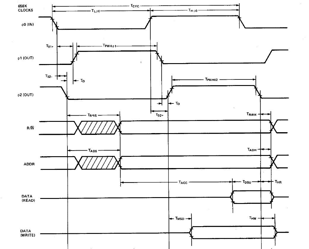
Very important: The 6502's cycle starts with the falling clock edge, then the processor sets up the address and R/W, well ahead of the rising edge of Φ2. Whether reading or writing, the data must be valid before the fall of Φ2 at the end of the cycle, with enough setup time for the data to be latched in at the falling edge. The timing diagrams in the data sheets have all the details.
One cycle:
One cycle:
Code: Select all
          _________
\________/         \
http://WilsonMinesCo.com/ lots of 6502 resources
The "second front page" is http://wilsonminesco.com/links.html .
What's an additional VIA among friends, anyhow?
The "second front page" is http://wilsonminesco.com/links.html .
What's an additional VIA among friends, anyhow?
Re: Micro programmed 6502-like CPU
GARTHWILSON wrote:
Very important: The 6502's cycle starts with the falling clock edge, then the processor sets up the address and R/W, well ahead of the rising edge of Φ2. Whether reading or writing, the data must be valid before the fall of Φ2 at the end of the cycle, with enough setup time for the data to be latched in at the falling edge. The timing diagrams in the data sheets have all the details.
One cycle:
One cycle:
Code: Select all
          _________
\________/ \In my particular implementation control signals (including R/W) change on the falling edge of Φ2, and data is latched on the rising edge.
The write cycle starts at point D, on the falling edge of Φ2. Addresses have been set on the preceding rising edge, so they should be valid by this point. R/W changes shortly after, so does the data, which is valid through E and to the falling edge of Φ2 in F, when it's latched by for example RAM.
The read cycle starts in A, with valid addresses and data set beforehand. The difference here is that data is read by the CPU on the rising edge of Φ2, on B instead of C. It has to be this way, as I'm latching data on the rising edge.
I suppose this would work, there would be plenty of setup time, unless the peripheral waits to the rising edge of Φ2 to output the data that is.
Juan
- Attachments
-
-
GARTHWILSON
- Forum Moderator
- Posts: 8775
- Joined: 30 Aug 2002
- Location: Southern California
- Contact:
Re: Micro programmed 6502-like CPU
Address must never change while Φ2 is high.
The peripheral will not even begin to output data until after the rise of Φ2 (except possibly in the case of ROM, depending on the glue logic); but it will have it ready ahead of the fall of Φ2.
Quote:
unless the peripheral waits to the rising edge of Φ2 to output the data that is.
The peripheral will not even begin to output data until after the rise of Φ2 (except possibly in the case of ROM, depending on the glue logic); but it will have it ready ahead of the fall of Φ2.
http://WilsonMinesCo.com/ lots of 6502 resources
The "second front page" is http://wilsonminesco.com/links.html .
What's an additional VIA among friends, anyhow?
The "second front page" is http://wilsonminesco.com/links.html .
What's an additional VIA among friends, anyhow?
Re: Micro programmed 6502-like CPU
I think I have gotten it right this time. I have added a couple flip flops and changed the microcode so signals change on the appropriate times. I had the phases swapped. Now it matches the timing diagram on WDC's datasheet. (I find this one easier to read: https://www.princeton.edu/~mae412/HANDOUTS/timing.bmp)
Juan
Juan
- Attachments
-
Re: Micro programmed 6502-like CPU
Rev A schematics are in! I'm sure there are plenty of typos and possible optimizations. I hope I can catch some of that during initial prototyping. Also attached a general block diagram. My design is horribly inefficient, but so far it works (on Logisim) and speed is not a requirement. I hope to make a functioning computer out of it. We'll see.
Juan
EDIT: Updated block diagram
Juan
EDIT: Updated block diagram
- Attachments
-
-
- REGISTERS CARD.pdf
- (257.61 KiB) Downloaded 121 times
-
- ALU CARD.pdf
- (342.34 KiB) Downloaded 123 times
-
- INTERFACE CARD.pdf
- (385.81 KiB) Downloaded 112 times
Last edited by JuanGg on Mon Jan 20, 2020 10:20 am, edited 1 time in total.

Re: Micro programmed 6502-like CPU
A milestone - well done!
I think sometimes it might help if you have a block diagram which shows the clock boundaries - perhaps something to consider.
I think sometimes it might help if you have a block diagram which shows the clock boundaries - perhaps something to consider.
Re: Micro programmed 6502-like CPU
Thanks! Updated the block diagram. Not sure if this is what you meant.
Juan
Juan