BigDumbDinosaur wrote:
rickseiden wrote:
The ACIA is addressed at $5000-$5FFF. I have two VIAs addressed at $6000-$6FFF and $7000-$7FFF. My ROM is $8000-$FFFF. My RAM is $0000-$3FFF.
Just an opinion, but that is a lot of wasted address space that could be used for more RAM. Have you considered using a 74*138 decoder to reduce the footprint of your I/O space? There is no reason for each I/O device to occupy 4KB of address space like that. You could arrange for the '138 to appear at $7000 and by connecting the A0-A2 inputs of the '138 to A8-A10, respectively, each piece of I/O hardware will occupy one page of address space. That allows you to reclaim space in which to address RAM.
Here's how I would do it if I were using your basic architecture:
Attachment:
simple_computer.gif
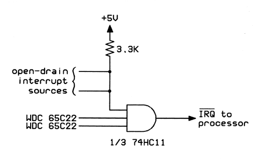
The above could be reduced to two chips by using the unused sections of the 74HC10 as substitutes for the 74HC00 NANDs. However, I drew it that way so you could better visualize the logic.
The selection logic for the UART and VIAs uses only their low-true select inputs, that is, CS2B on the VIAs and CS1B on the UART. The other select pins must be connected to Vcc. Almost all RAM and ROM has a /CE or similar for selecting the device. That is how I wired the RAM and ROM decoding.
At first I was really worried about all the empty space in my addressing scheme. Then I sat down and tried to write software for what I had built. IT WAS VERY DIFFICULT. Still is. So I'm not close to using what memory I have, meaning that it doesn't matter that I'm wasting it.
I did do some work on a closer addressing of devices. Like having one VIA be $6000-$600F and the next to $6010-$601F. It just took too many logic chips to do.
My board is modular, though. I have a main board with the CPU, ROM, RAM and the first VIA on it. Then I have the address lines fed out to a header on the left, and I've attached a small board with addressing logic on there, which in turn feeds back into the main board's chip select lines for the various chips. If I want to change my addressing scheme in the future, I just change that little side board. The second VIA and the ACIA are both on daughter boards that link in to headers on the side of the main board, and their addressing logic is on their boards. It does mean some redundancy in the chips, but it also means flexibility. Like I have one board that has just a VIA on it, and another board (that I probably need to redesign after today) that has a VIA and an ACIA on it, along with a CH340G chip and some USB headers so the USB to Serial is right on the board.
If I ever do anything more with this than just putz around--like as in design an actual computer or something--I'll clean it all up and put it all on one board. But for now, it's working out pretty well the way it is.


