Is it possible to overclock a 6502 to 100GHz
Re: Is it possible to overclock a 6502 to 100GHz
And packaging. How do you get the signals off that cell-sized CPU die?
Re: Is it possible to overclock a 6502 to 100GHz
Perhaps you could input and read with a tiny microwave generator? You`d build a tiny memory load and let the chip do something, wait, and then read. At first, it could be something like counting from 1 to 1 trillion in 10seconds.
Re: Is it possible to overclock a 6502 to 100GHz
Or, you could downlock for loading a program or reading something with an external device, using an amplifier, and overclock during the run of the program.
-
GARTHWILSON

- Forum Moderator
- Posts: 8775
- Joined: 30 Aug 2002
- Location: Southern California
- Contact:
Re: Is it possible to overclock a 6502 to 100GHz
MTd2, I/O will run at a small fraction of the umpteen-GHz processor clock speed. However, what Chromatix might have been getting at is that regardless of how small the circuit is, you'll still need space to bond the bondwires to, even if that were only power and ground and maybe a few other near necessities like a reset line. IOW, getting the processor (and the needed memory and other support) down to the size of a red blood cell does not mean you can make a die anywhere near that small.
http://WilsonMinesCo.com/ lots of 6502 resources
The "second front page" is http://wilsonminesco.com/links.html .
What's an additional VIA among friends, anyhow?
The "second front page" is http://wilsonminesco.com/links.html .
What's an additional VIA among friends, anyhow?

Re: Is it possible to overclock a 6502 to 100GHz
When going for small chip size and high speed, IMHO the best approach would be having 64kB RAM and some I\O on chip.
In other words: something like an improved version of the W65C134S "microcomputer".
Chips at the size of a red blood cell, now that would be something like Smartdust.
Hmm... feels like size\durability of the "batteries" required for keeping such tiny computers up and running would be going to be an interesting topic.

Re: Is it possible to overclock a 6502 to 100GHz
Ken Shirriff did one of his very interesting writeups on an RFID chip - four connections, very small indeed.
http://www.righto.com/2016/06/inside-ti ... s-san.html
Direct write to wafer - skipping masks - was a thing at one time. Still is, perhaps:
https://en.wikipedia.org/wiki/Maskless_lithography
Once again, anything not mainstream will fail to get the economies of scale which make chips so cheap.
(Chips no longer have blank areas on them: with modern processes, the whole rectangle must be patterned, so where there are not circuits there are filler patterns. So, no gain from trying to mix in white space with the chips - the mask is just as complex and will be just as expensive.)
Re: Is it possible to overclock a 6502 to 100GHz
On the topic of custom chips as a service, like PCBs, although there are possibilities for that, the obvious way to go is FPGA. You just ship the final design (the 'bitstream') on a serial EEPROM. At least one FPGA manufacturer used to offer a custom-chip service which used your final FPGA design to make an exactly equivalent hardwired chip, not sure if they still do.
One might want to make up a list of pros and cons as to why a custom chip might be preferable to an FPGA, or vice versa. The design process might well be very much the same: HDL, synthesis, place and route, timing checks, final simulation. Anyone who feels FPGA is a step too far for them might well be wrong - it's not that hard - and certainly if you can't face designing an FPGA, you won't get on well designing a chip.
Here's a custom chip project which targets MOSIS 0.6u process:
https://hackaday.io/project/12996-cmos-game-of-life
And here's a multi-project chip idea which aimed to share costs between projects:
https://hackaday.io/project/152709-itsy ... n-100-chip
Re: Is it possible to overclock a 6502 to 100GHz
Just scaling computing in terms instructions per seconds is too much rough of an approximation, but doing it anyway 6502 delivers 0.430 MIPS at 1.000 MHz https://en.wikipedia.org/wiki/Instructions_per_second and it matches AMD Phenom II X4 940. If you could do all components to fit inside something the size of a red blood cell, you could navigate until each to an individual cancer cell and destroy it.
-
barrym95838

- Posts: 2056
- Joined: 30 Jun 2013
- Location: Sacramento, CA, USA
Re: Is it possible to overclock a 6502 to 100GHz
MTd2 wrote:
... If you could do all components to fit inside something the size of a red blood cell, you could navigate until each to an individual cancer cell and destroy it.
Got a kilobyte lying fallow in your 65xx's memory map? Sprinkle some VTL02C on it and see how it grows on you!
Mike B. (about me) (learning how to github)
Mike B. (about me) (learning how to github)
Re: Is it possible to overclock a 6502 to 100GHz
In theory, using nanobots for destroying cancer cells sounds like a nice idea... but there are some real_life issues to this.
First, considering nowadays PCs:
Not all of them would be working perfectly after they are manufactured.
Not all of them would be always working in a "predictable way", and it might be getting worse over time.
Means after some time of operation, quite a few of the nanobots won't be working "according to the program" anymore,
and to prevent the cure from getting worse than the disease we would need a plan for extracting _all_ of the nanobots
out of the patient in time and in a reliable way.
Second, the red tape related to getting something certified in the health care sector.
After you successfully invented a cure for cancer and proved to the world it really works,
it might take 20 years until it's acknowledged/approved and paid by the health care insurances.
Re: Is it possible to overclock a 6502 to 100GHz
The 6502 would be used for controlling the movements of the small robot and collect data. I don't think you'd make them navigate to the tumor, but you'd link them to a catheter, by really tiny wires. The catheter would also isolate them from the local blood stream, and relay information to a larger computer outside the patient. The robots would drill the cells and kill the sick cells.
Re: Is it possible to overclock a 6502 to 100GHz
They seem to be a number of misconceptions on what reducing dimensions of size buys you. With each reduction, there is always some trade off where one of the physical laws of physics becomes the dominant limiter. Before 120 nm it was the capacitance of the transistors to the die. From there to about 40 nm it was the low gain of the P-channel transistors. From the P-channel were fixed by the fin-fets. At around 10 to 7 nm the problem is becoming the internal resistance of the interconnecting wires and even fin-fet has lost its shine. 14-10 nm is about the limit of practical I/O drive. Real world interconnect wires are about 100 ohms impedance. Even with voltage reduction, noise limits it are becoming more difficult to deal with I/O.
It seems that around 5GHz is about the lower limit of practical silicon use. Going below 10 nm doesn't help that. The thought of even a 10 gHz 6502 at 14 nm doesn't make sense. Remember, the Intel processors are not doing everything in a single cycle like the 6502 is. These processors that are doing this level are there because they use pipelining and speculative execution ( causing side band security leaks ). Having the processor fetch, decode, execute and store data like the 6502 does within one or two clock cycles at even 5 gHz doesn't even sound practical. There are too many limiting cases.
Dwight
Re: Is it possible to overclock a 6502 to 100GHz
Wikipedia says, the (empirical) atomic radius of Silicon is 111pm.
Considering this, 7nm is small indeed.
There would be a physical limit to how few atoms a trace on a chip could be narrow,
or to how few atoms are required for storing a Bit in a reliable way.
Considering this, 7nm is small indeed.
There would be a physical limit to how few atoms a trace on a chip could be narrow,
or to how few atoms are required for storing a Bit in a reliable way.

Re: Is it possible to overclock a 6502 to 100GHz
ttlworks wrote:
Not all of them would be working perfectly after they are manufactured.
Not all of them would be always working in a "predictable way", and it might be getting worse over time.
Not all of them would be always working in a "predictable way", and it might be getting worse over time.
Re: Is it possible to overclock a 6502 to 100GHz
The nanobots will be very small, no matter what you are going to do, it's inevitable that some of them will end up in the human body.
It would be close to impossible to track where they went, and what they are doing there.
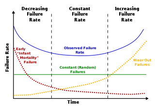
An "obstacle course" only would be useful in the first third of the bathtub curve.
Some sort of semiconductor material and metal would be required for building the nanobots.
While Silicium doesn't seem to be toxic, and Aluminium and Copper don't look too toxic,
I'm not sure about the long term effects of Silicides within the body.
If you are encapsulating the nanobots, it would be an interesting question what material to use.
Another interesting question would be, what the nanobots would be using as "batteries".
A possible solution would be injecting a new batch of nanobots into the patient once within a week for getting rid of any old nanobots.
Microsoft Nanohealth (TM) sure would keep you more healthy than average, but if you fail to pay for the weekly updates in time... well...
I'm not intentionally trying to spoil the party here, it's just that some points need to be put into consideration _before_ unleashing a new technology.
To run a useful discussion here, we would need to get academic degrees in semiconductor physics, chip design, nanomaterials, biochemistry etc. first.
It would be close to impossible to track where they went, and what they are doing there.
An "obstacle course" only would be useful in the first third of the bathtub curve.
Some sort of semiconductor material and metal would be required for building the nanobots.
While Silicium doesn't seem to be toxic, and Aluminium and Copper don't look too toxic,
I'm not sure about the long term effects of Silicides within the body.
If you are encapsulating the nanobots, it would be an interesting question what material to use.
Another interesting question would be, what the nanobots would be using as "batteries".
A possible solution would be injecting a new batch of nanobots into the patient once within a week for getting rid of any old nanobots.
Microsoft Nanohealth (TM) sure would keep you more healthy than average, but if you fail to pay for the weekly updates in time... well...
I'm not intentionally trying to spoil the party here, it's just that some points need to be put into consideration _before_ unleashing a new technology.
To run a useful discussion here, we would need to get academic degrees in semiconductor physics, chip design, nanomaterials, biochemistry etc. first.