Hi Jeff.
Nah, 'register renaming' in a Pentium is a lot worse.

;---
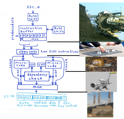
Now for a (hypothetical, over_simplified and half_baked) picture about what might happen if a 6502 might be trying to "go 68060":
//Some of the images in the picture are "borrowed" from wikipedia.
Attachment:
 6502_goes_68060.png [ 799.56 KiB | Viewed 1137 times ]
First we have the (8 Bytes) Instruction Buffer plus the two Byte shifters, fed from the (32 Bit) data bus.
//The Byte shifters could be implemented with a "lattice" of 74CBTLV245 chips.
Attached to (almost) every Byte in the Instruction Buffer we have a predecoder which mainly checks for the length of an instruction.
//Expect each predecoder to be at least 12 chips when checking the length of K24\65816 instructions.
Then some multiplexers for extracting all the Bytes for two 6502 CISC instructions.
//If you want to extract more than two instructions at 100MHz with 74LVC\74CBTLV chips, this needs to be pipelined.
Basically, something like a "bucket wheel excavator" which grinds into program memory for breaking it into single 6502 CISC instructions.Now that we have two "slots" containing the Bytes for two 6502 CISC instruction, we can't tell which of the instruction might finish first when getting executed.
This calls for something like two little buffers with 2:1 multiplexers in front of them for swapping the slots if needed.
//We need to keep track, in which order the instructions went in for doing a "dependency check" later.
//If we won't have this function block here, this would complicate the Instruction Buffer circuitry a lot.
Sort of a "shell game" with two 6502 CISC instructions.//Other superscalar CPUs implement a bigger buffer for a lot of "CISC instructions".
The two 6502 CISC instructions then are handled by two microcode blocks, every microcode block has a "state machine counter".
Each microcode block emits one set of µOPs for every machine cycle, that's something like vertical microcode.
The speed of the microcode storage might be a topic.We then need to check dependencies, how the µOPs would fit together.
Register usage, function block usage in the CPU, which CISC instruction went initiated first, etc.
//The dependency check mechanism has to tell the microcode counters, if a new µOP could be generated.
Might be something like hammering square pegs through round holes, plus something like
Lynn Conway's DIS.
A multiplexer (or a set of multiplexers) then "magically" puts together a VLIW word from all this (that part still isn't worked out).
It somehow reminds me to a meat grinder producing sausages.The VLIW word then is executed in the mill.;---
The picture leaves out a lot of little details:
Control signals between dependency check, microcode counters and Instruction Buffer circuitry.
How to handle conditional\unconditional changes in program flow.
How to put together the µOPs into a VLIW word.
What the VLIW word actually is supposed to look like.
...and maybe the list isn't complete.
The pipeline of the CPU might be ending up being 8 levels in total,
and the basic concept for handling interrupts and conditional\unconditional changes in program flow needs to be re_done.
;---
But my point here is:
If the CPU would support a "native VLIW mode" and we would be using sort of a compiler for static 6502 CISC to VLIW conversion,
with VLIW instructions being long word alligned, this might save us (a lot) more than 100 chips, this could keep the pipeline at 4 levels,
and all the complicated and probably bug ridden hardware for turning 6502 CISC into VLIW would fall out of the design
because then the compiler has to handle all this by software.