6502.org Forum  Projects  Code  Documents  Tools  Forum
It is currently Sat Nov 23, 2024 12:46 am

All times are UTC


Post new topic Reply to topic  [ 33 posts ]  Go to page 1, 2, 3  Next
Author Message
PostPosted: Sun Jun 09, 2019 2:05 pm 
Offline

Joined: Sun Jun 09, 2019 1:33 pm
Posts: 10
Hi there !

I'm a hobbist, and newbie in electronics.

I've an NMOS 6502 wired to a modern micro controller (a Teensy 3.6, running at 180 mhz)
Data bus, address bus, Phi1, Phi2, Phi0, Rw and RST are wired
RDY, NMI, IRQ are tied up to VCC with 5.1k resistors (I did not had the recommended 3K)
I've put a 10uF capacitor between GND and VCC near the Pin 1

I'm only doing things for the sake of understanding this old CPU that I used when I was a teen
The micro controller is there to simulate RAM/ROM access and generate the clock signal.

Using a cheap logic analyzer I can confirm that I've a 1MHZ clock signal fed to PHI0 with a duty cycle around 50%, probing at pin 37

Now, what I did is using a timer interrupt routine (on micro controller) at 2 MHZ
On each interrupt call I send a clock HI or a clock LOW, that's give me a 1MHZ signal with 50% duty - At least this is what Seleae Logic reports : 1 MHZ signal
From there I'm stuck I don't really understand the 6502 cycles, and spent countless hours on Google to read articles on this topic

I can't get the 6502 trying to read $FFFC/$FFFD after reset - All I get is garbage
So I don't know if I'm "sensing" the address bus at the right time

Here http://laughtonelectronics.com/Arcana/V ... iming.html
It seems that I need to wait for PHI2 to be high to read the address bus

From here https://lateblt.livejournal.com/88105.html
It seems that I need to wait for PHI2 to be high to read the address bus

I'm puzzled - I've tried to read the original 6502 specs but that's a little bit above my skills ;-)

I found some articles about 6502 wired to Arduinos, and those folks achieved some results more easily than me (no interrupt, simple loop()) whilst I can't get nothing but erratic behavior most of the time.

I know that the CPU must be reseted and what I simply do is

Code:
digitalWriteFast(SIG_RESET, LOW);
delay(50); // 50 milliseconds
digitalWriteFast(SIG_RESET, HIGH);


At program startup.

Facts :
- the whole project is on a breadboard (a low quality one)
- I tried to use short wires but some of them are still way too long (20 millimeters for some address bus bits)
- The 6502 is driven at 3.3v
- The 6502 should be an NMOS (that what I bought), how can I check if it's really an NMOS or a CMOS version ?
- 6502 CPU label is SY6502 / 8349 with Synertek logo
- The 6502 could be counterfait or broken ? I bought it from a well established French resealer (cost me under 7$)
- I don't know what I'm doing :-)
- I'm stuck to 3.3v, crafting a system with 3.3v on micro controller and 5v on 6502 is undoable for me (too complex)

Please, please any help appreciated I'm on the edge of the Full Frustration :-)

Top
 Profile  
Reply with quote  
PostPosted: Sun Jun 09, 2019 3:43 pm 
Offline
User avatar

Joined: Fri Aug 30, 2002 1:09 am
Posts: 8544
Location: Southern California
Welcome!

The NMOS 6502 is not guaranteed to work at 3.3V at all. It is a 5V device. Logic high at 3.3V is fine, but not power supply voltage.

The address and R/W lines will be valid before phase 2 rises.

You should find many of your questions answered in the 6502 primer, at http://wilsonminesco.com/6502primer/ .

_________________
http://WilsonMinesCo.com/ lots of 6502 resources
The "second front page" is http://wilsonminesco.com/links.html .
What's an additional VIA among friends, anyhow?


Top
 Profile  
Reply with quote  
PostPosted: Sun Jun 09, 2019 3:57 pm 
Offline
User avatar

Joined: Tue Mar 02, 2004 8:55 am
Posts: 996
Location: Berkshire, UK
I would start by generating the PHI2 clock in software from the ARM -- it makes it easier to tristate the data bus.

The logic I use in my three chip board is:
Code:

set ADDR BUS as input
set DATA BUS as input
set PHI2 output HI
set RESB output LO
set IRQB output HI
set R/W input

for 64 iterations
 set PHI2 LO
 delay 500nS
 set PHI2 HI
 delay 500nS
end-for
set RESB HI
delay

repeat
 set PHI2 LO
 set DATA_BUS input
 set PHI2 HI
 if R/W == READ
  set DATA_BUS output of RAM or ROM based on ADDR BUS value
  delay 500nS
 else
  if ADDR_BUS value is RAM
   RAM[ADDR BUS] = DATA BUS
  delay 500nS
forever


You can add in support for IRQs later.

_________________
Andrew Jacobs
6502 & PIC Stuff - http://www.obelisk.me.uk/
Cross-Platform 6502/65C02/65816 Macro Assembler - http://www.obelisk.me.uk/dev65/
Open Source Projects - https://github.com/andrew-jacobs


Top
 Profile  
Reply with quote  
PostPosted: Sun Jun 09, 2019 4:39 pm 
Offline

Joined: Mon May 21, 2018 8:09 pm
Posts: 1462
Given that you have a microcontroller running at 3.3V, I recommend upgrading to a CMOS version of the 6502, as that will also work at 3.3V and thus be easier to interface to your microcontroller.

I would also note that if you have an unsynchronised timer interrupt and are merely checking the state of the clock during its service routine, you have no guarantee whatsoever that the clock will *remain* high for the entire duration of your routine. Instead, you should have the Phi2 clock trigger interrupts on its rising and falling edges. Address lines will be valid on the rising edge, and data lines will be valid on the falling edge. You may need to switch the interrupt logic between rising and falling edges on each trigger, in which case you can direct it to separate service routines at the same time.


Top
 Profile  
Reply with quote  
PostPosted: Sun Jun 09, 2019 7:23 pm 
Offline
User avatar

Joined: Fri Aug 30, 2002 1:09 am
Posts: 8544
Location: Southern California
I took it to mean he has a timer interrupt on the microcontroller that hits two million times per second, and it flips the 6502's clock input each time, generating a 1MHz clock input, which is fine as long as the microcontroller emulating the other parts is fast enough to make them play nicely with that clock rate, meeting the setup times.

_________________
http://WilsonMinesCo.com/ lots of 6502 resources
The "second front page" is http://wilsonminesco.com/links.html .
What's an additional VIA among friends, anyhow?


Top
 Profile  
Reply with quote  
PostPosted: Mon Jun 10, 2019 8:38 am 
Offline
User avatar

Joined: Thu Dec 11, 2008 1:28 pm
Posts: 10986
Location: England
Welcome! Certainly you need to reconcile your CPU choice and your voltage. The Teensy 3.5 runs at 5V, so that's another way to get the Teensy and the 6502 working together. Using your Teensy 3.6 with a modern CMOS 6502 is also a good idea - especially if you can be extra-sure of getting a genuine working part.


Top
 Profile  
Reply with quote  
PostPosted: Mon Jun 10, 2019 9:44 am 
Offline

Joined: Sun Jun 09, 2019 1:33 pm
Posts: 10
Thanks a lot for your answers, I'm not alone anymore :-) But now I have more questions and I must rephrase some points of my initial post

Wilson, I know http://wilsonminesco.com/6502primer and theses pages are very valuable, I've read most of them during the last weeks but I still struggle to understand all the articles

1) Just to be sure about the signal names
PHI0 is the clock input, pin 37 - This one is an OUTPUT on MCU side and generated by the MCU (interrupt routine or not)
PHI1 is PHI0 inverted, pin 3 - This is an INPUT on MCU side
PHI2 is PHI0 with a slight propagation delay, pin 39 - This is an INPUT on MCU side

2) Andrew, about the pseudo code

When I started this experiment, I did not used any interrupt routine - I just tried to experiment with the main() loop even like many hobbyist did with slow Arduinos but most of the time I only got erratic behavior from the 6502.
In the pseudo code you use PHI2, so I presume you're talking about clock OUTPUT on MCU side, the signal that is fed on pin 37, should I stop using PHI0 as a valid term and stick with PHI1 and PHI2 (no matter if I speak about pin 39 or pin 37 ?

What is the first loop for ?
Code:
for 64 iterations
 set PHI2 LO
 delay 500nS
 set PHI2 HI
 delay 500nS
end-for
set RESB HI


I understand the RESET, but not the loop : Is it to stabilize the CPU before entering the main loop ?

Then, in the main loop
Code:
set PHI2 LO
set DATA_BUS input
set PHI2 HI


That means
- Generate clock LO
- Generate clock HI
- Then during clock HI I should have access to ADDR BUS, DATA BUS and R/W provided that I have the right nano seconds delays

The delay is a problem, the MCU is very very fast and the core might optimize the code execution so well that I did not found a way (I mean an article on the web) to have nano seconds delay using assembly "NOP". Not related with the 6502 but I should try to find a solution, may be putting a pin HIGH and LOW with NOP instructions in between and check the elapsed time with my chinese logic analyzer

I see that you set IRQ to HI, I presume it's the same that happen when IRQ pin is tied to VCC through a 5K resistor ?

Last point : I discovered the concept of "tri-state" few days ago and it confuses me a lot. 0, 1 and something else (the famous HI-Z) - Is tri state concept important/necessary to drive the 6502 ? Should I try again to understand what tri-state is ?

3) Chromatix

Yes, I'm aware that some NMOS 6502 could have problems with 3.3v - I will switch to the 65C02 in last resort, because I dream about partially emulating an old NMOS 6502 computer (an Oric Atmos) and may be the ROM original code could not run with a 65C02.
While typing the line above I did a quick search and found that using a 65C02 in an Oric Atmos is possible : http://forum.defence-force.org/viewtopi ... 44&p=19622
So that might change my plans ;-)

About the clock remaining HI see below

4) Interrupt flip flop
GARTHWILSON wrote:
I took it to mean he has a timer interrupt on the microcontroller that hits two million times per second, and it flips the 6502's clock input each time, generating a 1MHz clock input, which is fine as long as the microcontroller emulating the other parts is fast enough to make them play nicely with that clock rate, meeting the setup times.


Yes, this is how it works.
Pseudo code is
Code:
if flag
  write HI to PHI0
  read address bus
  store address value to volatile v_addr variable
  // The operations below are not yet implemented because until now my main concern is having $FFFC/$FFFD on addr bus which I never got with the interrupt routine (and very few times otherwise)
  read RW signal
  if RW is READ
    write RAM/ROM content on data bus
    store TRUE to volatile v_read_operation variable
  else
    write data bus content to RAM
    store FALSE to volatile v_read_operation variable
else
 write LO to PHI0
toggle flag


I arranged the connections between the 6502 pins and the MCU pins so I can read/write D0..D7 in one operation, read A15..A8 in one operation, read A7..A0 in one operation + 3 bits logical instructions
So it's pretty fast.

Then on the main loop I would

Code:
loop
  cli // disable interrupts
  copy v_addr and v_read_operation to local variables
  sei
  emulate simple things (keyboard, text mode ?)


If the code in the main loop is fast enough that could work.
BTW I should try to find an ARM disassembly tool that can give me cycle timing for each assembly instruction.
And I should do some maths to correlate the 180MHZ speed of the MPU and the 2MHZ interrupt to determine the maximum nano seconds I can spend in one main loop iteration

5) Last notes

- I already have two versions of the code, one with an interrupt timer, one without so I can easily check Andrew's pseudo code provided I can wait for nano seconds

From http://laughtonelectronics.com/Arcana/V ... iming.html
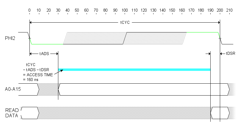
When the 6502 wants to read from memory
Image
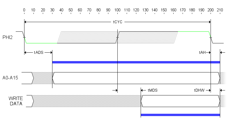
or when the 6502 wants to write to memory
Image

In both cases the address bus is valid when PHI2 is high so I don't need any delay
But I need a few nano seconds delay before I read or write to the data bus, or am I wrong and there's no need to wait at all ?


Thanks again for your help, I hope this post is not too much confuse ;-)


Top
 Profile  
Reply with quote  
PostPosted: Mon Jun 10, 2019 11:35 am 
Offline

Joined: Sun Jun 09, 2019 1:33 pm
Posts: 10
BigEd wrote:
Welcome! Certainly you need to reconcile your CPU choice and your voltage. The Teensy 3.5 runs at 5V, so that's another way to get the Teensy and the 6502 working together. Using your Teensy 3.6 with a modern CMOS 6502 is also a good idea - especially if you can be extra-sure of getting a genuine working part.


I missed your post ;-) Took me 60 minutes to write mine...

Yes, I thought about the T3.5 but it runs at 120 MHZ, that 60MHZ less than the T3.6 might be a problem if I'm very tight on timing resources, even if both of them can be overclocked the T3.6 win in all cases

About being extra sure if a 65C02 or 6502 is a genuine one, it's hard to say nowadays, so many ebay and amazon vendors, online suppliers, shops...


Top
 Profile  
Reply with quote  
PostPosted: Mon Jun 10, 2019 3:58 pm 
Offline
User avatar

Joined: Thu Dec 11, 2008 1:28 pm
Posts: 10986
Location: England
It might be worth a more careful study of Jeff's diagrams. Part of the message about 6502 timing is that the Phi2 rising edge is not a timing reference. It can be useful but nothing is defined relative to it.

When you are supplying data to the 6502, you need to read the address bus late enough that you know it has finished changing, and to drive the data bus early enough that you know the 6502 has time to capture the correct final value when phi2 falls. And then to stop driving the data bus rather soon after phi2 falls.

When you are reading data from the 6502, you need, again, to read the address bus late enough, but this time you need to read the databus late enough that you know it's finished changing. One approach, when you're in the place of a microcontroller running code to emulate a peripheral, is to read both the clock and the databus repeatedly, and then to use the latest databus value which corresponds to phi2 being high.


Top
 Profile  
Reply with quote  
PostPosted: Mon Jun 10, 2019 7:51 pm 
Offline
User avatar

Joined: Fri Aug 30, 2002 1:09 am
Posts: 8544
Location: Southern California
tactif-cie wrote:
In the pseudo code you use PHI2, so I presume you're talking about clock OUTPUT on MCU side, the signal that is fed on pin 37. Should I stop using PHI0 as a valid term and stick with PHI1 and PHI2 (no matter if I speak about pin 39 or pin 37?

For current-production 65c02's, WDC prefers that you use only the pin-37 input as the timing reference. The internal hardware is still there and operational for pins 3 and 39 but they no longer test or guarantee the timings for them. For older 6502's and 65c02's, it was normal to reference everything from pin 39.

Quote:
What is the first loop for ?
Code:
for 64 iterations
 set PHI2 LO
 delay 500nS
 set PHI2 HI
 delay 500nS
end-for
set RESB HI


I understand the RESET, but not the loop. Is it to stabilize the CPU before entering the main loop?

The CPU needs several clock cycles during the reset-low time to get itself ready for business. Just holding the reset line down without cycling the clock is not enough.

Quote:
Then on the main loop I would

Code:
loop
  cli // disable interrupts
  copy v_addr and v_read_operation to local variables
  sei
  emulate simple things (keyboard, text mode?)

Correction on CLI and SEI: CLI stands for "CLear Interrupt-disable bit," meaning you will now allow interrupts. SEI stands for "SEt Interrupt-disable bit," meaning that now you will not accept interrupts. Be aware however that setting the interrupt-disable bit is an automatic part of the reset and interrupt sequences already; so you don't have to do an SEI at the beginning.

Quote:
BTW I should try to find an ARM disassembly tool that can give me cycle timing for each assembly instruction.
And I should do some math to correlate the 180MHz speed of the MPU and the 2MHz interrupt to determine the maximum nanoseconds I can spend in one main loop iteration

This is a normal part of any realtime software design.

Quote:
In both cases the address bus is valid when PHI2 is high so I don't need any delay
But I need a few nanoseconds delay before I read or write to the data bus, or am I wrong and there's no need to wait at all?

The address bus, R/W, and SYNC are guaranteed to be valid and stable the tADS time after phase 2 falls, which makes them available before phase 2 rises. However, when the processor is writing (ie, R/W is low), the data it is sending out on the data bus is not guaranteed to be valid until tMDS after the rise of phase 2. If your microcontroller reads the data bus right after the rise of phase 2, you will get invalid data.

_________________
http://WilsonMinesCo.com/ lots of 6502 resources
The "second front page" is http://wilsonminesco.com/links.html .
What's an additional VIA among friends, anyhow?


Top
 Profile  
Reply with quote  
PostPosted: Thu Jun 13, 2019 10:38 am 
Offline

Joined: Sun Jun 09, 2019 1:33 pm
Posts: 10
Before giving up with the NMOS at 3.3v and ordering a 65C02, I would really appreciate your advice about the code of my interrupt service routine. Can you see something I do the wrong way ?

Meaningful code blocks are

On micro controller start :

Code:
pinMode(SIG_RESET, OUTPUT);
pinMode(SIG_CLOCK, OUTPUT);
pinMode(SIG_RW, INPUT);

for (int i = 0; i < 16; i++)
        pinMode(addr_pins[i], INPUT);

init_isr(); // From there a signal clock is generated (see ftm0_isr() below)
delay(100); // Give time (100 ms) to the cpu before reset
digitalWriteFast(SIG_RESET, LOW);
delay(1000); // 1 second
digitalWriteFast(SIG_RESET, HIGH);


Then the isr (for now it's running at 1MHZ so that's 500KHZ for the 6502) :

Code:
FASTRUN void ftm0_isr(void) {
    uint16_t addr_lo, addr_hi;
    uint32_t port;

    FTM0_SC &= ~FTM_SC_TOF; // clear the interrupt overflow flag
    GPIOC_PDDR = 0x00;      // Set data bus in input mode, let the 6502 drive the bus
    if (isr_flag) {
        GPIOE_PDOR |= (1 << 24); // Put PHI2 HI
        // tADS has endured from LO cycle : RW and ADDR are guaranteed
        rw = (GPIOE_PDIR & 0x4000000) >> 26; // Pin 24
        addr_lo = GPIOD_PDIR & 0xFF;         // 5, 21, 20, 6, 8, 7, 13, 2
        port = GPIOB_PDIR;                   // 32, 31, 30, 29, 1, 0, 17, 16
        addr_hi = port & 0x03;               // 17, 16
        addr_hi += (port & 0xF0000) >> 14;   // 30, 29, 1, 0
        addr_hi += (port & 0xC00) >> 4;      // 32, 31
        addr = (addr_lo << 8) + addr_hi;
        if (rw) {                    // 6502 wants to read an address location
            GPIOC_PDDR = 0xFFFFFFFF; // Set data bus in output mode
            GPIOC_PDIR |= ram[addr]; // Write memory to data bus
        } else {                     // 6502 wants to write to an address location
            P3;                      // 18 NOPs Is it enough at 180MHZ for tMDS ? Should we wait more / less ? How much ?
            P3;
            ram[addr] = GPIOC_PDIR & 0xFF; // Write data bus to memory
        }
    } else {
        GPIOE_PDOR &= ~(1 << 24); // Put PHI2 LO
    }
    isr_flag = !isr_flag;
}


Once again, thanks for your help and time !


Top
 Profile  
Reply with quote  
PostPosted: Sat Jun 22, 2019 1:22 pm 
Offline

Joined: Sun Jun 09, 2019 1:33 pm
Posts: 10
I switched to a CMD G65SC02, the behavior of the cpu seems more reliable, even if it's still not ok because now I'm facing another problem :

VCC is 3.3v
The emulated ram contains only NOPs (EA) opcodes
The NMI, RDY and IRQ pins are tied up to VCC through 4.7K resistors

After RESET the cpu never tries to read from $FFFC/$FFFD but endlessly tries to read $FFFE/$FFFF and I don't understand why

Extract of output (first row is R/W)

Code:
1 0000
1 0001
0 011A
0 0119
0 0118
1 FFFE
1 FFFF
1 0000
1 0001
0 0117
0 0116
0 0115
1 FFFE
1 FFFF
1 0000
1 0001
0 0114
0 0113
0 0112
1 FFFE
1 FFFF
1 0000
1 0001
0 0111
0 0110
0 010F
1 FFFE
1 FFFF
1 0000
1 0001
0 010E
0 010D
0 010C
1 FFFE
1 FFFF
1 0000
1 0001
0 010B
0 010A
0 0109
1 FFFE
1 FFFF
1 0000
1 0001
0 0108
0 0107
0 0106
1 FFFE
1 FFFF
1 0000
1 0001
0 0105
0 0104
0 0103
1 FFFE
1 FFFF
1 0000
1 0001
0 0102
0 0101
0 0100
1 FFFE
1 FFFF
1 0000
1 0001
0 01FF
0 01FE
0 01FD
1 FFFE
1 FFFF
1 0000
1 0001
0 01FC
0 01FB
0 01FA
1 FFFE
1 FFFF


Top
 Profile  
Reply with quote  
PostPosted: Sat Jun 22, 2019 1:29 pm 
Offline
User avatar

Joined: Thu Dec 11, 2008 1:28 pm
Posts: 10986
Location: England
Looks like the CPU is always reading zeros - it's reading 0000 for the vector and then reading 00 which is a BRK as the opcode.


Top
 Profile  
Reply with quote  
PostPosted: Sat Jun 22, 2019 2:00 pm 
Offline

Joined: Sun Jun 09, 2019 1:33 pm
Posts: 10
I just checked again, $FFFE/$FFFF contains EA so the 6502 should jump to EAEA address and that never happen

I'm certainly doing something wrong, but I really don't see where is the mistake - I checked all the wires, checked again my interrupt routine, port reading and writing

I suspect a problem related with bad timings for databus write/read. I might be reading or writing the databus too early or too late when I put PHI2 on HIGH state

Code:
READ  EA from FFFE
READ  EA from FFFF
READ  EA from 0000
READ  EA from 0001
WRITE 00 to   018E
WRITE 02 to   018D
WRITE 77 to   018C
READ  EA from FFFE
READ  EA from FFFF
READ  EA from 0000
READ  EA from 0001
WRITE 00 to   018B
WRITE 02 to   018A
WRITE 77 to   0189
READ  EA from FFFE
READ  EA from FFFF
READ  EA from 0000
READ  EA from 0001
WRITE 00 to   0188
WRITE 02 to   0187
WRITE 77 to   0186
READ  EA from FFFE
READ  EA from FFFF
READ  EA from 0000
READ  EA from 0001
WRITE 00 to   0185
WRITE 02 to   0184
WRITE 77 to   0183
READ  EA from FFFE
READ  EA from FFFF
READ  EA from 0000
READ  EA from 0001
WRITE 00 to   0182
WRITE 02 to   0181
WRITE 77 to   0180
READ  EA from FFFE
READ  EA from FFFF
READ  EA from 0000
READ  EA from 0001
WRITE 00 to   017F
WRITE 02 to   017E
WRITE 77 to   017D
READ  EA from FFFE
READ  EA from FFFF
READ  EA from 0000
READ  EA from 0001
WRITE 00 to   017C
WRITE 02 to   017B
WRITE 77 to   017A
READ  EA from FFFE
READ  EA from FFFF
READ  EA from 0000
READ  EA from 0001
WRITE 00 to   0179
WRITE 02 to   0178
WRITE 77 to   0177
READ  EA from FFFE
READ  EA from FFFF
READ  EA from 0000
READ  EA from 0001
WRITE 00 to   0176
WRITE 02 to   0175
WRITE 77 to   0174


Top
 Profile  
Reply with quote  
PostPosted: Sat Jun 22, 2019 2:04 pm 
Offline
User avatar

Joined: Thu Dec 11, 2008 1:28 pm
Posts: 10986
Location: England
When phi2 falls, the 6502 reads the databus. So the value needs to stay there for some ten or tens of nanoseconds.


Top
 Profile  
Reply with quote  
Display posts from previous:  Sort by  
Post new topic Reply to topic  [ 33 posts ]  Go to page 1, 2, 3  Next

All times are UTC


Who is online

Users browsing this forum: No registered users and 13 guests


You cannot post new topics in this forum
You cannot reply to topics in this forum
You cannot edit your posts in this forum
You cannot delete your posts in this forum
You cannot post attachments in this forum

Search for:
Jump to: