I'm a hobbist, and newbie in electronics.
I've an NMOS 6502 wired to a modern micro controller (a Teensy 3.6, running at 180 mhz)
Data bus, address bus, Phi1, Phi2, Phi0, Rw and RST are wired
RDY, NMI, IRQ are tied up to VCC with 5.1k resistors (I did not had the recommended 3K)
I've put a 10uF capacitor between GND and VCC near the Pin 1
I'm only doing things for the sake of understanding this old CPU that I used when I was a teen
The micro controller is there to simulate RAM/ROM access and generate the clock signal.
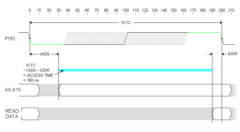
Using a cheap logic analyzer I can confirm that I've a 1MHZ clock signal fed to PHI0 with a duty cycle around 50%, probing at pin 37
Now, what I did is using a timer interrupt routine (on micro controller) at 2 MHZ
On each interrupt call I send a clock HI or a clock LOW, that's give me a 1MHZ signal with 50% duty - At least this is what Seleae Logic reports : 1 MHZ signal
From there I'm stuck I don't really understand the 6502 cycles, and spent countless hours on Google to read articles on this topic
I can't get the 6502 trying to read $FFFC/$FFFD after reset - All I get is garbage
So I don't know if I'm "sensing" the address bus at the right time
Here http://laughtonelectronics.com/Arcana/V ... iming.html
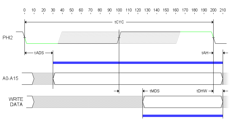
It seems that I need to wait for PHI2 to be high to read the address bus
From here https://lateblt.livejournal.com/88105.html
It seems that I need to wait for PHI2 to be high to read the address bus
I'm puzzled - I've tried to read the original 6502 specs but that's a little bit above my skills
I found some articles about 6502 wired to Arduinos, and those folks achieved some results more easily than me (no interrupt, simple loop()) whilst I can't get nothing but erratic behavior most of the time.
I know that the CPU must be reseted and what I simply do is
Code: Select all
digitalWriteFast(SIG_RESET, LOW);
delay(50); // 50 milliseconds
digitalWriteFast(SIG_RESET, HIGH);
Facts :
- the whole project is on a breadboard (a low quality one)
- I tried to use short wires but some of them are still way too long (20 millimeters for some address bus bits)
- The 6502 is driven at 3.3v
- The 6502 should be an NMOS (that what I bought), how can I check if it's really an NMOS or a CMOS version ?
- 6502 CPU label is SY6502 / 8349 with Synertek logo
- The 6502 could be counterfait or broken ? I bought it from a well established French resealer (cost me under 7$)
- I don't know what I'm doing
- I'm stuck to 3.3v, crafting a system with 3.3v on micro controller and 5v on 6502 is undoable for me (too complex)
Please, please any help appreciated I'm on the edge of the Full Frustration