I'm new to 6502 & 6502 forum and want to build my first 6502 SBC. My prototype board is ROMless. It has a battery-backed RAM, an Altera EPM7128S CPLD and prototype area for a 5V DIP 8-bit processors such as 6502. The CPLD contains a serial port that can be setup to receive 255 bytes of serial data and write it into RAM and then release the control to the processor. I image such bootstrap scheme has been done before and there are discussions, schematic & software already for it? I'd appreciate a link to that. Thank you!
Bill
Serial bootstrap

Re: Serial bootstrap
plasmo wrote:
The CPLD contains a serial port that can be setup to receive 255 bytes of serial data and write it into RAM
BTW -- welcome, plasmo !
-- Jeff
In 1988 my 65C02 got six new registers and 44 new full-speed instructions!
https://laughtonelectronics.com/Arcana/ ... mmary.html
https://laughtonelectronics.com/Arcana/ ... mmary.html

Re: Serial bootstrap
plasmo wrote:
I'm new to 6502 & 6502 forum and want to build my first 6502 SBC. My prototype board is ROMless. It has a battery-backed RAM, an Altera EPM7128S CPLD and prototype area for a 5V DIP 8-bit processors such as 6502. The CPLD contains a serial port that can be setup to receive 255 bytes of serial data and write it into RAM and then release the control to the processor. I image such bootstrap scheme has been done before and there are discussions, schematic & software already for it? I'd appreciate a link to that. Thank you!
Bill
Bill
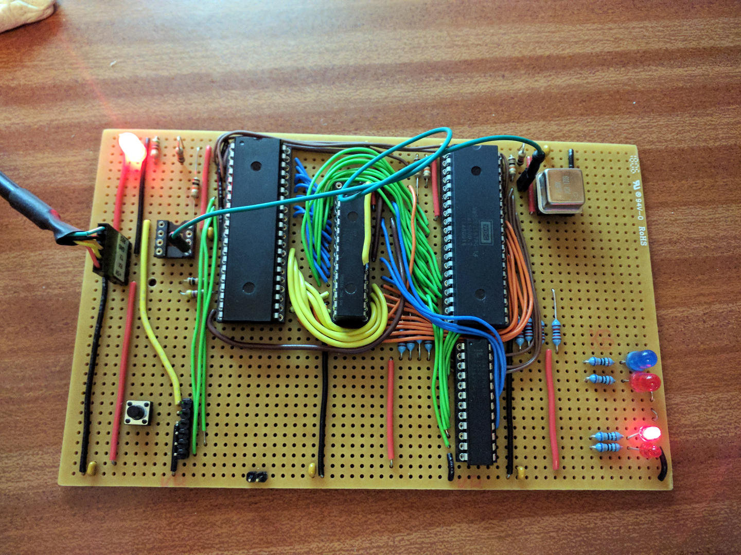
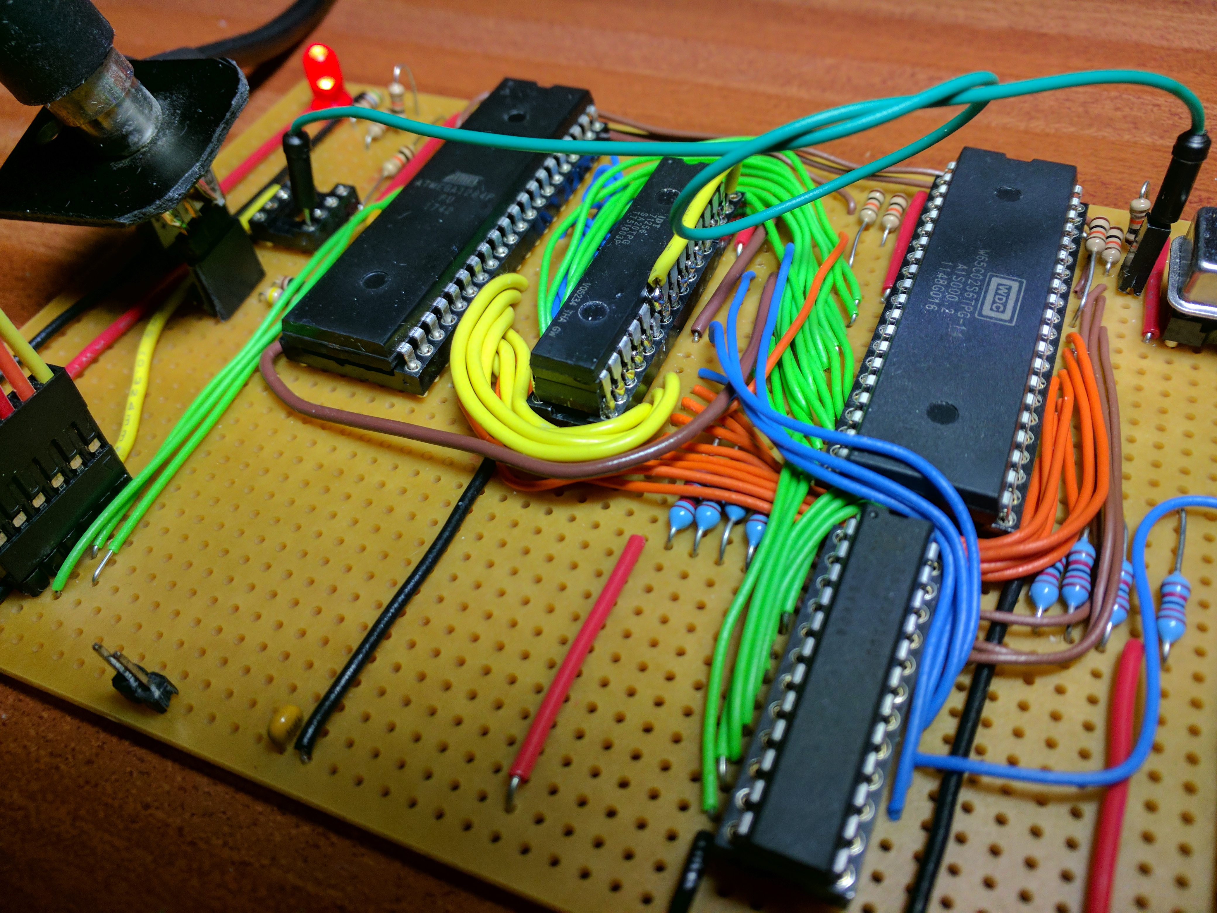
The ATmega uses 2 x 8-bit ports for the bottom 8 address lines and the data bus. I tristate them when not in-use. It also controls the Reset, BE, RW and Rdy lines. (the latter is read and write). The top 8 address lines are pulled high.
So to boot the 6502, the ATmega halts the 6502 (Reset, Rdy and BE low), writes about 200 byes of first stage bootstrap into the top 256 byes of RAM, pokes the reset vector (to $FF00), tristates the AD ports, lifts BE and Rdy and then lifts Reset - the 6502 Boots, then it communicates with the ATmega via that shared area of RAM (Writes commands into it, executes WAI, the ATmega, having the Rdy pin in read mode, senses it going low, takes BE low, reads the command, updates the RAM, sends an IRQ to the 6502 which terminates the WAI and off the 6502 goes. so once the 6502 is boots the ATmega acts like a UART, video output device and a ROM based filing system (working on sticking an SD card into it).
Pictures here: https://unicorn.drogon.net/ruby-02.jpg and here: https://unicorn.drogon.net/IMG_20181115_164041.jpg
And welcome to the wonderful world of the 6502!
-Gordon
--
Gordon Henderson.
See my Ruby 6502 and 65816 SBC projects here: https://projects.drogon.net/ruby/
Gordon Henderson.
See my Ruby 6502 and 65816 SBC projects here: https://projects.drogon.net/ruby/

Re: Serial bootstrap
We've had a number of threads touching on this bootstrapping problem. My own preference is for the first code loaded to be able to read srec format hex, with which you can load a more fully featured monitor. But it's enough for the first stage bootstrap to be able to accept addresses and data for a series of single-byte writes.
Bruce did write a wonderful single-page monitor but it turns out to be for the 65Org16, a homebrew CPU which bears a family resemblance to the 6502. Could be a useful reference though: Other threads which have touched on this topic:
Bruce did write a wonderful single-page monitor but it turns out to be for the 65Org16, a homebrew CPU which bears a family resemblance to the 6502. Could be a useful reference though: Other threads which have touched on this topic:
- Demonstration of bootstrapping a ROMless machine (not 6502)
Bootstrapping an SBC (21 or 22 bytes of bootstrap)
Another Bootstrap for a ROM less system
Simplest self-contained project
Instructions all in ram?
6502 with a serial port - a minimal monitor?
Ultra-minimal 3-wire Interface boots up 65xx CPU's
Last edited by BigEd on Sat Dec 07, 2019 9:26 am, edited 2 times in total.
Re: Serial bootstrap
There are some interesting & clever ideas discussed in these threads! Frankly, the tightly-coupled multiprocessors approach is too difficult for me, I'm having enough problem dealing with just one processor! The other interesting bootstrap method (3-wire interface) is heavily dependent on the 6502 operating characteristics and there may not be an equivalent function in Z80/6809/8085. My larger goal is to develop a generic 8-bit processors development platform for Z80/680x/808x/1802/6502 and even 16-bit processors with 8-bit data bus like 68008/32008.
The serial bootstrap is inspired by Z280's UART bootstrap mode. The complexity of 5V CPLD are limited so I simplified the concept and implemented it in a modest CPLD. There is a hybrid printed-wiring/wire-wrapped prototype board based on the concept:
https://www.retrobrewcomputers.org/doku ... lasmo:g8pp
A Z80 SBC is a spin off of the design:
https://www.retrobrewcomputers.org/doku ... o:z80sbc64
Bill
Re: Serial bootstrap
With a sufficiently new 65C02, you get a "VP" (vector pull) signal which, in combination with decoding of low-order address lines, would allow you to reliably intercept the Reset or NMI vector in hardware, without also having to decode the other address lines. You could then hold RDY low until the bootstrap code has been received and written to RAM (assuming you do all that sequencing in hardware), and then simply output the 16-bit entry address of the code just written.
I plan to use a similar scheme to implement a front-panel for bootstrapping my project, eliminating the need for any dedicated EEPROM programmer.
I plan to use a similar scheme to implement a front-panel for bootstrapping my project, eliminating the need for any dedicated EEPROM programmer.
Re: Serial bootstrap
Having read a bit about 6502 boot sequence, I plan to hold 6502 in reset and BE low while in serial bootstrap mode, which will tri-state the address/data/control signals. A8-A15 will be driven high and I will send 255 bytes of serial data which will be written to RAM from address 0xFF00 to 0xFFFE. When the 255th serial data is received, the CPLD will negate reset and BE; 6502 starts running from reset vector at 0xFFFC. The reset vector points to first stage boot loader starting from 0xFF00 which is a small S-record loader to load & run 2nd stage monitor. The monitor have a command to copy itself into bootstrap area so it will boot up when in RAM bootstrap mode. I also need to protect the monitor from alteration by subsequent software by switch it to a hidden bank. Will this work? Are there software convention where ROM, RAM, I/O and system variables are typically located?
Bill
Bill
Re: Serial bootstrap
This sounds good! (The idea of protecting the monitor from overwrites is in the nature of a safety feature: if it works, great, but it isn't absolutely necessary.)
The 6502 itself pretty much forces ROM to the top of the memory map (for the vectors) and RAM to the bottom (for zero page and stack). So I/O generally lands somewhere in the middle. With minimal decoding you get large blocks assigned, so I/O might end up at $8000. With fine grained decoding, I/O could be kept to a single page, such as $FE00 (overlaying some of the ROM).
At one extreme, you have just 64 bytes of RAM, and at the other extreme, 64k-512 bytes of RAM. Or even a little more.
Re: Serial bootstrap
plasmo wrote:
Having read a bit about 6502 boot sequence, I plan to hold 6502 in reset and BE low while in serial bootstrap mode, which will tri-state the address/data/control signals. A8-A15 will be driven high and I will send 255 bytes of serial data which will be written to RAM from address 0xFF00 to 0xFFFE. When the 255th serial data is received, the CPLD will negate reset and BE; 6502 starts running from reset vector at 0xFFFC. The reset vector points to first stage boot loader starting from 0xFF00 which is a small S-record loader to load & run 2nd stage monitor. The monitor have a command to copy itself into bootstrap area so it will boot up when in RAM bootstrap mode. I also need to protect the monitor from alteration by subsequent software by switch it to a hidden bank. Will this work? Are there software convention where ROM, RAM, I/O and system variables are typically located?
Bill
Bill
I never bothered to protect any RAM in my system - just write careful code
You'll need some mechanism to communicate back to the outside world - so you either use the window with the CPLD or stick a separate UART on the 6502 - if going down the latter route note that the current new 65C51 UART has a bug in it and you'll need to use software timing for the Tx port. (Maybe you can emulate a memory mapped UART in the CPLD?)
As for conventions for rom/ram/io - it's up to you, but the 6502 needs RAM at the bottom of memory (you need RAM in page 0 and 1 for anything other than a tiny trivial program), ROM at the top (because of the vectors), and IO somewhere in-between. My system has the 256 byte shared buffer at FFxx, IO is at FExx, my mini OS is at F000 up to a max. of FDFF and RAM from 0000-EFFF. (so 60KB) I have nothing more than an 8-bit latch + LEDs for IO right now (Rev B on the PCB has a 6522). I only use 128 bytes of the shared buffer for comms with the host though, so fetching a file is done in 128 byte chunks. No big deal - it loads 16K of BBC Basic in about a second,
-Gordon
--
Gordon Henderson.
See my Ruby 6502 and 65816 SBC projects here: https://projects.drogon.net/ruby/
Gordon Henderson.
See my Ruby 6502 and 65816 SBC projects here: https://projects.drogon.net/ruby/
Re: Serial bootstrap
During serial bootstrap, CPLD is a DMA device taking over 6502 bus; all these signals need to be tri-statable when 6502 resumes control.
Is 4K ROM enough for a decent monitor? Does ROM typically swapped out and replaced with RAM? I don't have ROM, but if ROM are typically swapped out and replaced with RAM, then I also need to swap out the boot-able RAM page and replace with another RAM page, so I don't have to serially bootstrap every time. I can memory map 0xEF00 to 0xEFFF to I/O devices; below that is nearly 60K of RAM.
The same serial port for bootstrap function is also normally a simple serial port with 2 memory locations (data, status). It is hardwired to 115200, N81 so there is no configuration/control registers. Additional I/O expansion is possible through the RC2014 connector. Is there a well-known disk OS (like CP/M) that interface to compact flash? Is banked memory normally done in the 6502 world? I imagine a real-time clock is a good thing to have even if it is just a DS1302 with bit-bang interface.
Bill
Re: Serial bootstrap
plasmo wrote:
During serial bootstrap, CPLD is a DMA device taking over 6502 bus; all these signals need to be tri-statable when 6502 resumes control.
Is 4K ROM enough for a decent monitor? Does ROM typically swapped out and replaced with RAM? I don't have ROM, but if ROM are typically swapped out and replaced with RAM, then I also need to swap out the boot-able RAM page and replace with another RAM page, so I don't have to serially bootstrap every time. I can memory map 0xEF00 to 0xEFFF to I/O devices; below that is nearly 60K of RAM.
The same serial port for bootstrap function is also normally a simple serial port with 2 memory locations (data, status). It is hardwired to 115200, N81 so there is no configuration/control registers. Additional I/O expansion is possible through the RC2014 connector. Is there a well-known disk OS (like CP/M) that interface to compact flash? Is banked memory normally done in the 6502 world? I imagine a real-time clock is a good thing to have even if it is just a DS1302 with bit-bang interface.
Bill
Is 4K ROM enough for a decent monitor? Does ROM typically swapped out and replaced with RAM? I don't have ROM, but if ROM are typically swapped out and replaced with RAM, then I also need to swap out the boot-able RAM page and replace with another RAM page, so I don't have to serially bootstrap every time. I can memory map 0xEF00 to 0xEFFF to I/O devices; below that is nearly 60K of RAM.
The same serial port for bootstrap function is also normally a simple serial port with 2 memory locations (data, status). It is hardwired to 115200, N81 so there is no configuration/control registers. Additional I/O expansion is possible through the RC2014 connector. Is there a well-known disk OS (like CP/M) that interface to compact flash? Is banked memory normally done in the 6502 world? I imagine a real-time clock is a good thing to have even if it is just a DS1302 with bit-bang interface.
Bill
4K? Woz did his original monitor in under 256 bytes... (google WozMon) My little OS stub is currently 2.5K but it has a lot of text and code to emulate enough of a BBC Micro to make BBC Basic work. What do you want out of a "monitor"?
ROM swapped for RAM - some systems can do that, some simply copy ROM into RAM (typically RAM can be faster if you need to generate wait states for old/slow ROM) However you don't have ROM, so not sur why you're even worrying about it.
There is a 6502 CP/M lookalike OS - although I don't think anyone actually uses it. See: http://www.z80.eu/dos65.html
Banked memory? Sure - google for BBC Micro + sideways RAM/ROM. RTC? If you need it... The BBC has 32K RAM, then 16K of ROM which was stacked up to 8 ROMs high, so you could switch in any one of those ROMs - so Basic would reside in one, the disk filing system in another, wordprocessor in the next, Logo, etc. and so on. The Operating System (in the top 16K minus some for hardware IO) managed the ROMs and communication between them. Latterly RAM boards came on the scene and you could load images from disk, and the last revision (the BBC Master) had side-ways RAM as standard.
In the laste 70's/early 80's, there were also plug-in cards for the Apple II to give more RAM and the (ill-fated) Apple /// also had banked RAM, so it's not a new concept.
Soooooo.... I think you may need to sit down and work out what you really want and what you're going to do with it... I' d suggest starting with as simple a system as possible. Run some code on it (ie. get that serial bootloader going) then make plans...
FWIW: My Ruby 6502 system is so-called because it's a bit of a nostalgia trip - I first wrote code for the 6502 40 years ago and back then I built several small 6502 SBC type systems for industrial control, so it's a bit of nostalgia for me, although I'm looking at retro style hardware but with todays knowledge re. software and applications.. And while I have something that might resemble a "monitor" it's really just a debugging aid and will be replaced by a more operating system-ey thing when I get more time.
Cheers,
-Gordon
--
Gordon Henderson.
See my Ruby 6502 and 65816 SBC projects here: https://projects.drogon.net/ruby/
Gordon Henderson.
See my Ruby 6502 and 65816 SBC projects here: https://projects.drogon.net/ruby/
Re: Serial bootstrap
I'm sure the experienced assembly programmers can write very compact code, but newbie like myself may have a repertoire of a dozen instructions and try to do everything with that thus inefficient code.
Just try to anticipate what may come down the road as I get going. Having programmable logic does give me quite a bit of flexibility, and my board is indeed very simple, just RAM, 6502, oscillator and CPLD. so I probably should get going and see what happens next.
Thanks everyone for the tips to get me started.
Bill
-
floobydust

- Posts: 1394
- Joined: 05 Mar 2013
Re: Serial bootstrap
Monitor space really depends on how many functions you plan to have in your monitor and how detailed any text based messages are. For my current C02 Pocket SBC, I reserved the top 2KB for BIOS and I/O and the next 6KB for the monitor (total of 8KB at the top of addressing). Simple memory map is:
$0000-$7FFF - 32KB RAM
$8000-$FDFF - EEPROM
$FE00-$FE9F - 5-I/O selects 32 bytes wide
$FEA0-$FFFF - EEPROM
Monitor starts at $E000 and BIOS starts at $F800.
So far the BIOS and I/O is less than 1KB and the Monitor is a little over 4KB, but I do have a fair amount of functions between the BIOS and Monitor. In addition to the usual memory operations (display, move, fill, compare, execute) and register operations, I have code that supports writing to the EEPROM insitu, a full disassembler that supports all WDC opcodes/addressing modes, timer/counter support for delays, benchmarking and a realtime clock, a Xmodem download utility with S19 record support and separate JUMP tables for both the Monitor and BIOS. There's some other stuff in there too, but that's the bulk of it.
Only a few things left to add... a Xmodem uploader, a simple assembler and the ability to do enter single-byte patching of the EEPROM. I also added the ability to launch EhBasic recently. Overall, it's reasonably sized for all of the functions that are in there.
BTW - Looked at your links... very interesting project!
Regards, KM
https://github.com/floobydust
https://github.com/floobydust
Re: Serial bootstrap
One option for the memory map would be to look closely at the Acorn Second Processor modules, which could be hung off the side of a BBC Micro using an interface called the "Tube". The idea was that the BBC Micro would handle the graphics, keyboard, disks and so on, while the Second Processor was where the application would actually run - with almost a full 64KB RAM to work with and nearly double the clock speed (3.5MHz) of the original machine. The MOS API was implemented, partly locally in the Second Processor's firmware, and partly through communication with the BBC Micro, such that normal BBC software could run if written "correctly". A special version of BBC BASIC was provided which could be "loaded high", giving the maximum amount of space for BASIC programs to use.
This was achieved by mirroring a tiny and very slow 2KB ROM under the top of RAM. A full 64KB RAM array was provided, but on reset the top 2KB was "hidden" so that reads in that area were instead serviced by the ROM. To accommodate the slow access time of the ROM, the clock speed of the CPU was severely restricted, down to about 200kHz I think. The first job of the Reset handler in that ROM was to read and then immediately rewrite every byte of itself, thereby transferring itself in-place into the top 2KB of RAM. It would then trigger the hardware to map out the ROM and crank up to full clock speed. There was also a small I/O carve-out - I think 32 bytes - within that 2KB area, which contained the Tube interface, and the "rewrite" routine had to skip over that.
With modern SRAM and EEPROM chips, the hack of changing clock speeds isn't needed any more, but a slow EEPROM might benefit from the correct use of RDY.
Re: Serial bootstrap
Is there a trick to tri-state the address/data/control bus of W65C02? The documentation indicates that pulling BE low will cause the address/data/control bus to tri-state, but poking around the chip with a scope, it doesn't seem to do it. Pulling RDY low along with BE helps somewhat, but address lines appear to be driven still.
I want to tri-state W65C02 immediately after reset so a DMA device can take over the bus and fill the RAM with bootstrap code but the CPU does not appear to release the bus because I can only drive addresses to 2V and current consumption rises dramatically up to 300mA depending on how many address lines are in contention.
Bill