Firstly, try swaping TXD and RXD, just in case you have them around the wrong way. Also check the baud rate, the source code should tell you what this is set to, it'll also depend on the clock running correctly. Check baud, parity, stop bits and confirm that putty has the same values as the source code specifies. I'd also try a simple loopback test to confirm everything is working on the computer side. Just connect TXD to RXD from the CP2102, open up putty and start typing, it should echo your characters back.
CP2102 works. I tried both the method you described and I had a router laying around that I hooked it up to. Baud rate, parity, and stop bits are set to what the source code specifies (115200 baud, 8 bits, hardware handshake, no parity, 1 stop bit)
I'd also recheck all the connections and make sure there are no wiring mistakes. If you have a multimeter check all the 5v and GND pins and make sure they are reading correctly.
Working on this now. Unfortunately I I don't have much in the way of equipment, but in a little bit I'll be back at my alma mater where I can probably make use of one of the oscilloscopes in the labs.
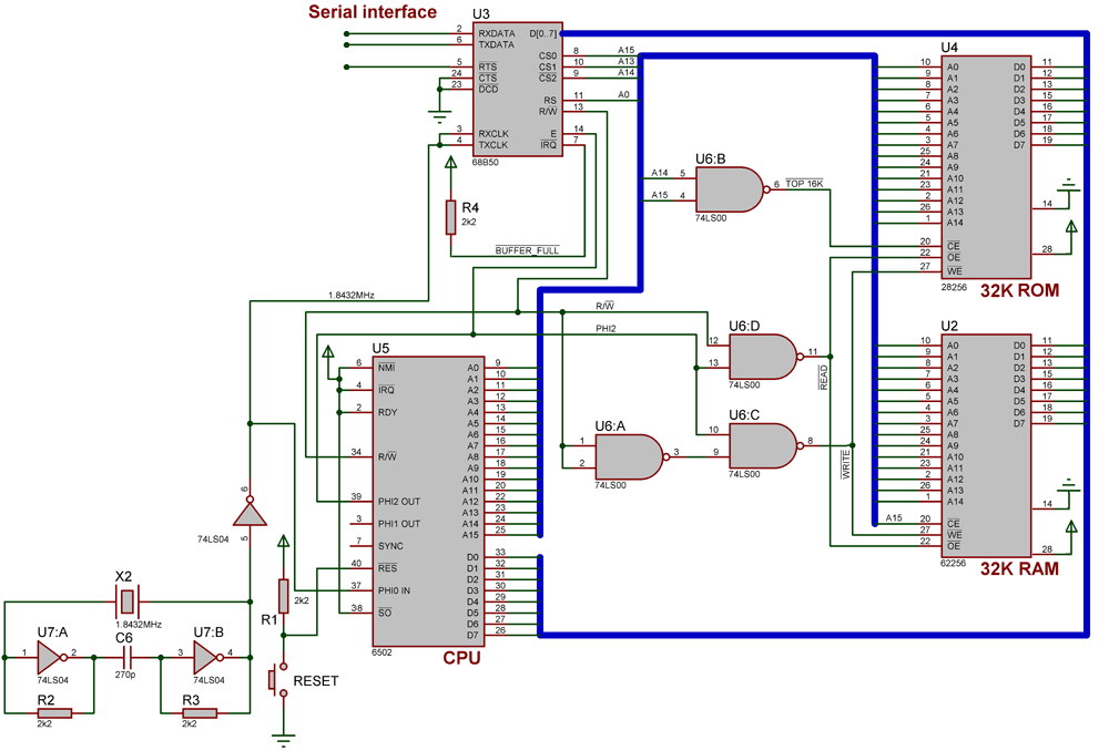
We can probably assume that the code is fine, but it would pay to check that you have burned the ROM correctly (using a verify step on your programmer) and that the code is built for the same memory map that you have (specifically the address of the 68B50.
I'll check on this and report back.
I just noticed you are using a WDC 65C02, this may be a problem as they don't recommend using PHI2 OUT (I think). Try using the clock signal directly instead of PHI2 in the address decode.
Made this change on the breadboard and it doesn't seem to be the (only) issue. Thanks for letting me know though!
That's quite a bit to get started with, maybe it would be helpful if you let us know what testing tools you have, such as a multimeter, oscilloscope, logic probe etc.
I appreciate the suggestions! As I mentioned, I'll double check the code matches the memory map, and soon enough I'll have access to an oscilloscope which should help make this less of a shot in the dark.