6502.org Forum  Projects  Code  Documents  Tools  Forum
It is currently Tue Sep 24, 2024 5:24 am

All times are UTC


Post new topic Reply to topic  [ 122 posts ]  Go to page Previous  1, 2, 3, 4, 5, 6 ... 9  Next
Author Message
PostPosted: Tue Oct 09, 2018 1:24 pm 
Offline
User avatar

Joined: Mon May 25, 2015 2:25 pm
Posts: 642
Location: Gillies, Ontario, Canada
A very observant question!

When you consider the legal levels for a TTL logic high of 2.7-5.0 volts and the legal level for a CMOS high of 3.5-5.0 volts, there could be a potential error of .8 volts. Since VRW is always sending to JetPack, this is a problem.

In an early design, I tried a direct connection, and it actually worked on several VIC-20's I connected. On others, my Kernal would crash within about 10 seconds of operation. Also note that, I will later use VRW on other parts of the board, so I am not just speaking about the single 245 on the Data Line shown here.

So my rule is that any TTL -> CMOS must be buffered by the Level Translating HCT logic.

The extra 8-10ns of propagation is no issue at all. In fact, it works in my favor as you will see as I move ahead. The Address and Data lines are later switched by another 245, so this extra delay puts all signals right back into alignment.

Depending on the path of Address and Data on the final design, I may actually direct connect VRW to the DIR pin on the DATA.245, but will still buffer the VRW as it is hown here for the rest of the board.

Brad

floobydust wrote:
Very nice start... however, I'm just wondering... any particular reason you didn't simply run the V/RW line directly to the Dir pin on the databus 245 transceiver versus running it through another 245 first? I can see having a buffered line to your bus, but not switching the databus direction through an additional delay.


Top
 Profile  
Reply with quote  
PostPosted: Tue Oct 09, 2018 3:24 pm 
Offline
User avatar

Joined: Wed Aug 17, 2005 12:07 am
Posts: 1228
Location: Soddy-Daisy, TN USA
Oneironaut wrote:
my Kernal would crash


Thanks for using the *CORRECT* spelling of KERNAL in Commodore lingo. ;-)

_________________
Cat; the other white meat.


Top
 Profile  
Reply with quote  
PostPosted: Tue Oct 09, 2018 3:32 pm 
Offline
User avatar

Joined: Mon May 25, 2015 2:25 pm
Posts: 642
Location: Gillies, Ontario, Canada
Updated the IO Buffer Schematic shown in the last page.
The 74HC08 AND gate is used to combine all four 8K segments into one large 32K segment.

Becaue one of the 8K segments lives in "Block5", the VIC-20 will boot from there.

In the final design, I have a small "Kernal" program that boots the VIC (like a game cartridge).
This Kernal sets up the VIC registers as well as the screen into 184x176 Bitmap mode.

To add some really cool retro tech, I will probably have the Kernal stored in a Diode Matrix!

Brad


Top
 Profile  
Reply with quote  
PostPosted: Tue Oct 09, 2018 7:18 pm 
Offline
User avatar

Joined: Mon May 25, 2015 2:25 pm
Posts: 642
Location: Gillies, Ontario, Canada
The next breadboard work to be done will look like this...

Image
Boot Loader and Frame Memory Switch.

Since I am posting small images, here is a better size for viewing...
http://lucidscience.com/temp/jps1l.jpg

The circuit above will perform several functions. First, it will boot the VIC on Block.5 (Address 40960), which is the standard method for autoloading a VIC-20 cartridge. This small Kernal Boot program just sets up the VIC internal registers, formatting the screen as a 184x176 color bitmap (actually 92x176 multicolor).

After that, the Kernal jumps to Address 8192 (Block.1), where a complex sequence of instructions and data are streamed to the VIC (24K worth). This "Frame Data" is assigned as 4900 blocks of 5 instructions each. This Frame Data is very specific to the Raster Line Timing, and can generate a shear-free animation at 30 frames per second. More on that later. Addresses to this memory are generated by 74HC163 counters, controlled by special bits stored in the Frame Control Memory.

The Frame Data is split into two components; Instructions and actual Data. These two components are switched over to the Data Bus by the bits stored in the Frame Control Memory. The 74HC157 Data Selectors swap between data destined for the 6560 and actual frame control instructions. A 5 byte block of Frame Data may look like this...

Code:
Byte 0 : LDA (Frame Memory)
Byte 1 : Pixel Data (Dual Data Memory)
Byte 2 : STA (Frame Memory)
Byte 3 : Screen ADR.LO (Frame Memory)
Byte 4 : Screen ADR.HI (Frame Memory)


In my testing, I found that I can do any task from drawing pixels to setting sound registers with this 5 byte blocking of Frame Data. Some of this data will be static per frame, and some will be dynamic at 30 fps.

The "Dual Data Mem Black Box" represents a large amount of ICs, that split memory into 8 bits or 2 bits of data depending on how it is accessed. More on that later, but here is a snapshot of what one half of that memory will look like...

Image
One Half of the Double Buffered Frame Data Memory.

The switched memory scheme shown above (half) allows the VIC to read 23*176 (8 Bits) of data as screen character data while the JetPack GPU writes to the other half as a 92*176 (2 Bits) four color bitmap. So this is basically a dual buffer video memory that adapts between chunky and 2 bit packed mode. The entire circuit is just a duplicate of what is shown, but with the Flip bits inverted. VIC is always reading one buffer (character and color data) as the JetPack GPU wites to the other.

Also note that the Kernal ROM will be a massive Diode Matrix, just because I think it would be cool.
I will now back off on schematic design and start building some real hardware!

Later.
Radical Brad


Top
 Profile  
Reply with quote  
PostPosted: Tue Oct 09, 2018 9:46 pm 
Offline
User avatar

Joined: Thu Dec 11, 2008 1:28 pm
Posts: 10938
Location: England
Would like to see a huge diode matrix - but can you make a fast one??


Top
 Profile  
Reply with quote  
PostPosted: Wed Oct 10, 2018 12:34 am 
Offline
User avatar

Joined: Mon May 25, 2015 2:25 pm
Posts: 642
Location: Gillies, Ontario, Canada
Indeed I can!
1N914's feeding 74HC245s as rows with 74HC138's energizing columns.
There will be six 138's generating 32 columns of 8 bytes, for a total Boot Code of 256 bytes.

I expect such a configuration to respond at least as well as the required 977.77 nanosecond access time.
But then again, I won't know until I try.

Brad

BigEd wrote:
Would like to see a huge diode matrix - but can you make a fast one??


Top
 Profile  
Reply with quote  
PostPosted: Wed Oct 10, 2018 6:02 am 
Offline
User avatar

Joined: Fri Nov 09, 2012 5:54 pm
Posts: 1429
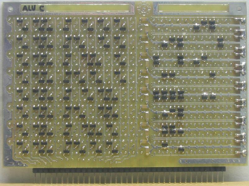
Many years ago, I had built that MT15 transistor CPU.
Did use transistorised PLAs for the instruction_decoder\sequencer.
//That sort of PLA in CTL technology requires pull_down transistors at the outputs.

Image

In that time frame, I had an idea for a ROM from BC847\BC857 transistors in my backhead, but it never went built.

Those transistors might be in the same price range as diodes nowaday,
the advantage when using transistors instead of diodes is the current gain of the transistors,
means one would have to worry a lot less about fan_in\fan_out issues and capacitances,
making it less difficult to build fast _and_ big ROMs.

The idea basically circled around making "bigger PLAs":
First to make a 'master file' for the PLA schematic and PCB layout with _all_ of the NPN transistors present.
To have a script for the PCB layout software which takes a copy of the 'master files' and marks NPN transistors
in the schematic and layout as "not to be soldered into the PCB" according to a binary file.
Then to tell the PCB manufacturer to solder the parts into the PCBs according to the modified PCB layout.
Some PCB manufacturers would do this for a fair price...
...and when pulling some tricks a C64 Kernal + Basic probably might fit into a shoe box.

Downside is, that 16kB of "discrete ROM" might drain more than 5A from a 2.5V power supply,
power consumption depends on the resistance of the pull_up\pull_down resistors in the ROM,
and of course that resistance has to be a compromise between ROM speed and power consumption.

IMHO it would make more sense to build a 256 Byte ROM containing a bootloader instead of building a 16kB ROM
containing Kernal + Basic.


Top
 Profile  
Reply with quote  
PostPosted: Wed Oct 10, 2018 6:05 am 
Offline
User avatar

Joined: Thu Dec 11, 2008 1:28 pm
Posts: 10938
Location: England
Oh, a proper two-plane PLA! Very nice.


Top
 Profile  
Reply with quote  
PostPosted: Wed Oct 10, 2018 6:29 am 
Offline
User avatar

Joined: Fri Nov 09, 2012 5:54 pm
Posts: 1429
Thanks, Ed.

Since I had the feeling that it would become neccessary to change the PLAs during debugging,
and I didn't want to solder a lot of tiny SMD transistors into and out of the PCBs,
I had added a solder jumper for every transistor at the bottom of the PCB:

Image

So it would have been possible to solder in _all_ of the transistors,
then to "program" the PLA by just opening/closing these "jumpers" with a solder iron.

Before making the PLA PCB layout, I had spent some time with paper and pencil to figure out
how to arrange/place the components to make a compact layout for a PCB with two layers.

BTW: For a 2.5V powered two input AND\OR CTL combination gate with low impedance resistors like in MT15,
we could expect a propagation delay slightly below 5ns, that's nearly 74F08 speed.
//Propagation delay for BC847\BC857 based differential ECL is ca. 20ns.

Other hobbyists use BC847\BC857 (SMD version of BC547\BC557) low_frequency transistors for building relay drivers and audio amplifiers. ;)


Top
 Profile  
Reply with quote  
PostPosted: Wed Oct 10, 2018 1:13 pm 
Offline
User avatar

Joined: Mon May 25, 2015 2:25 pm
Posts: 642
Location: Gillies, Ontario, Canada
This is very cool, thanks for sharing!
I first have to decide how JetPack is going to boot.

Option 1...
A small 128-256 byte KickStart just setsup the VIC and then jumps over to address 8192 in Block.1. At that point the game logic in the external cartridge will be responsible for formating the 24K Frame Memory from 8192 to 32767.

Option 2...
An 8K ROM (Block 5) is used that boots the VIC, and then does all Frame Memory formating. An initial 4K Bitmap (Startup Logo) and some sond would also be present to give the unit a little bling on startup.

Option 1 is a bit simpler and could use a Diode Matrix.
Option 2 gives the unit a more refined feel with a boot screen and allows future ROM changes.

I will decide over the weekend.

Brad


Top
 Profile  
Reply with quote  
PostPosted: Wed Oct 10, 2018 4:19 pm 
Offline
User avatar

Joined: Mon May 25, 2015 2:25 pm
Posts: 642
Location: Gillies, Ontario, Canada
Once again, all of my domain pointers are dead.
I am back on a support ticket.
Odd. Assigns are all good, but nothing points.
Until then, my images are all dead.
Frickin' modern tech!

** Problem resolved **
Had to reassign all domain pointers and rebuild web.config
Why?... who knows!

Brad


Top
 Profile  
Reply with quote  
PostPosted: Thu Oct 11, 2018 5:32 am 
Offline
User avatar

Joined: Fri Nov 09, 2012 5:54 pm
Posts: 1429
Oneironaut wrote:
Frickin' modern tech!

Fast\reliable web server plus Ethernet controller built from 1980s logic parts sure would be a cool project. :)

Modern tech sure is powerful... and small... and inexpensive... but it tends to emenate that odd Mickey Mouse smell.


Top
 Profile  
Reply with quote  
PostPosted: Thu Oct 11, 2018 3:08 pm 
Offline
User avatar

Joined: Mon May 25, 2015 2:25 pm
Posts: 642
Location: Gillies, Ontario, Canada
That would be a fun project.
It would be a challeng to do any better than Dennis Kuschel's MyCPU project...

http://www.mycpu.eu/

Brad

ttlworks wrote:
Oneironaut wrote:
Frickin' modern tech!

Fast\reliable web server plus Ethernet controller built from 1980s logic parts sure would be a cool project. :)

Modern tech sure is powerful... and small... and inexpensive... but it tends to emenate that odd Mickey Mouse smell.


Top
 Profile  
Reply with quote  
PostPosted: Thu Oct 11, 2018 3:20 pm 
Offline
User avatar

Joined: Thu Dec 11, 2008 1:28 pm
Posts: 10938
Location: England
See also Magic-1:
Quote:
Magic-1 is a completely homebuilt minicomputer. It doesn't use an off-the-shelf microprocessor, but instead has a custom CPU made out of 74 Series TTL chips. Altogether there are more than 200 chips in Magic-1 connected together with thousands of individually wrapped wires. And, it works. Not only the hardware, but a full software stack. There's a ANSI C cross-compiler for Magic-1 (retargeted LCC), a fully multi-user, multi-tasking port of the Minix 2 operating system. a TCP/IP stack and hundreds of programs.


Top
 Profile  
Reply with quote  
PostPosted: Thu Oct 11, 2018 3:52 pm 
Offline
User avatar

Joined: Wed Aug 17, 2005 12:07 am
Posts: 1228
Location: Soddy-Daisy, TN USA
That Magic-1 is amazing. I'd love to have some card cages like that too.

_________________
Cat; the other white meat.


Top
 Profile  
Reply with quote  
Display posts from previous:  Sort by  
Post new topic Reply to topic  [ 122 posts ]  Go to page Previous  1, 2, 3, 4, 5, 6 ... 9  Next

All times are UTC


Who is online

Users browsing this forum: No registered users and 57 guests


You cannot post new topics in this forum
You cannot reply to topics in this forum
You cannot edit your posts in this forum
You cannot delete your posts in this forum
You cannot post attachments in this forum

Search for:
Jump to: