6502.org Forum  Projects  Code  Documents  Tools  Forum
It is currently Tue Apr 30, 2024 5:14 pm

All times are UTC


Post new topic Reply to topic  [ 45 posts ]  Go to page 1, 2, 3  Next
Author Message
PostPosted: Thu Aug 02, 2018 2:57 am 
Offline
User avatar

Joined: Thu May 28, 2009 9:46 pm
Posts: 8160
Location: Midwestern USA
Something that I have been closely studying is the topic of wait-state generation. My interest is fueled by the desire to get my POC V2 unit to run as fast as possible (20 MHz would be great). POC V2 has a number of hardware features that complicate wait-stating, and units built by some others here may well have the same characteristics. Before continuing, please note that this discussion is specific to the WDC versions of the 65C02 and 65C816. My theories should be applicable to non-WDC 65C02s, but as I don't have anything powered by one of those processors, I can't prove that to be the case.

The 6502 family since inception has had the RDY input to stop the processor for an arbitrary amount of time. In simple terms, as long as RDY is held high the MPU will run and execute instructions. When RDY is brought low the MPU will stop, with a caveat—the NMOS family does not respond to RDY during a write cycle. In the case of the WDC MPUs, negating RDY causes the MPU to stop on the next high-to-low Ø2 transition—the MPU's internal clock will remain in the high state once it has stopped. When RDY has been driven high the MPU will restart on the next high-to-low Ø2 transition.

While RDY is low and the MPU is stopped, all registers will be maintained in the state they were in at the time RDY was driven low. Also, all outputs, such as the address bus, RWB, etc., will be maintained as though the Ø2 clock had been stopped in the high phase. Implied by this is the 65C816 will be using the data bus for data purposes, not extended addressing. There is no limit as to how long the MPU can be stopped with RDY.

Some interesting design problems can arise with the use of RDY for wait-stating. Consider the following circuit, which is used to generate read and write signals for hardware that have separate /OE (output-enable) and /WE (write-enable) inputs:

Attachment:
File comment: Ø2-Qualified Read/Write Circuit
read_write_qualify_alt.gif
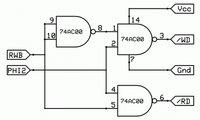
read_write_qualify_alt.gif [ 46.98 KiB | Viewed 12939 times ]

In studying the above circuit's logic, it can be seen that neither /RD (read data) or /WD (write data) can be driven low ("asserted") unless Ø2 (netlist symbol PHI2) is high, which is when the data bus would have valid content. That's all well and good—until the MPU is stopped with RDY. Although the MPU will maintain the state of RWB (high if reading, low if writing) while halted, the above circuit will "malfunction." Each time Ø2 goes low, /RD or /WD will be de-asserted, and when Ø2 goes high again, asserted. The potential for the addressed device to get confused by the oscillating /RD or /WD signal will be high.

Another case in which trouble can arise is one in which Ø2 is used to qualify chip selects, for example:

Attachment:
File comment: Ø2-Qualfied Decoding Circuit
wilson_decode.gif
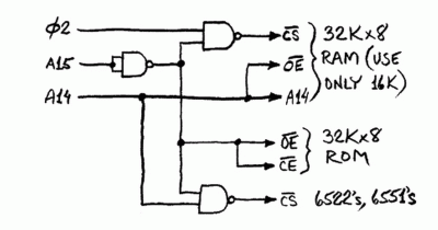
wilson_decode.gif [ 174.81 KiB | Viewed 12939 times ]

The above circuit was copied from Garth Wilson's website. Note the chip select (/CS) to the RAM, which is not asserted unless Ø2 is high and A15 is low. If A15 is low while the MPU has been wait-stated with RDY, that chip select will synchronously oscillate with Ø2, causing the RAM to be repeatedly deselected and selected.

A third case that is specific to the 65C816 is the generation of the A16-A23 address bits, which appear on the data bus during Ø2 low. Here's an example generator circuit:

Attachment:
File comment: 65C816 A16-A23 Address Generation
extended_address_generation.gif
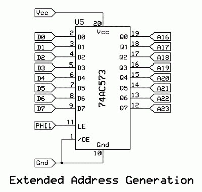
extended_address_generation.gif [ 24.63 KiB | Viewed 12939 times ]

During Ø2 low (PHI1 high), the eight latches in the 74AC573 octal D-type transparent latch will be opened, causing the Q outputs to follow the D inputs. Since it is during Ø2 low that the 65C816 emits the bank bits, the Qs will reflect the bank address. When Ø2 makes a low-to-high transition, the latches will close and the '573 will maintain the extended address on its Qs. At the same time, the 65C816 will cease driving the bank bits onto D0-D7 and instead will start treating D0-D7 as a data bus.

If after latching the bank address, the MPU is stopped with RDY, an unfortunate situation will arise on the next fall of Ø2. The '573 will open its latches, again causing the Qs to follow the Ds. However, the data bus at that time will reflect data, not bank bits, and when Ø2 goes high again and the latches close, A16-A23 will contain the data bus bit patterns, not the previously-captured bank bits, resulting in a wrong address being given to the system.

Given the above scenarios (and there are some others that are similar), it almost seems as though use of RDY will create problems, not solve them, particularly if a 65C816 is powering the system. During the design of my POC V2.2 unit, I came to the realization that any attempt at wait-stating involving the use of RDY would run into two of the above cases, and I would have a unit that would not properly operate. That realization caused me to stop design work and cogitate on developing a good method of wait-stating.

As I noted above, the 'C02 and '816 internally stop their clocks in the high phase upon responding to a low on RDY. A corollary to that characteristic is to be found in a small note buried in the data sheet:


    PHI2 can be held in either high or low state to preserve the contents of internal registers since the microprocessor is a fully static design.

The above is from the 65C02 data sheet. The 65C816 data sheet has a similar note:

    PHI2 can be held in either state to preserve the contents of internal registers and reduce power as a Standby mode.

In other words, it is possible to halt either MPU without detriment by simply halting the clock. Since a wait-state induced via negation of RDY halts the MPU in the Ø2 high phase, it can be surmised that externally stopping Ø2 in the high phase should accomplish the exact same thing as using RDY. However, since it would be the clock generator that would be stopped, not just the MPU, anything slaved to the clock, such as the aforementioned read/write, chip select, and extended address circuits, would likewise stop and maintain their state.

Hence the objective will be to concoct a glitch-free method of halting Ø2 in the high phase and simultaneously halting Ø1 in the low phase. Just how would this be accomplished? I'll present my ideas in the next post.

_________________
x86?  We ain't got no x86.  We don't NEED no stinking x86!


Last edited by BigDumbDinosaur on Sun Oct 24, 2021 7:10 pm, edited 3 times in total.

Top
 Profile  
Reply with quote  
PostPosted: Thu Aug 02, 2018 4:56 am 
Offline

Joined: Mon May 21, 2018 8:09 pm
Posts: 1462
An alternative strategy would be to construct Phi2R and Phi1R signals that are qualified by RDY, and use those for qualification of /OER & /WER for slow devices, bank-select, etc. That is:
Code:
Phi1R = (~Phi2 & RDY) = ~(Phi2 | ~RDY)
Phi2R = ~(~Phi2 & RDY) = (Phi2 | ~RDY)
/OER = ~(R/W & Phi2R) = ~(R/W & ~(Phi2 | ~RDY))
/WER = ~(~R/W & Phi2R) = (R/W | (~Phi2 & RDY))

Fast memory devices not requiring wait-states should still use directly Phi2 qualified /OE and /WE signals, to avoid the extra gate delay involved in constructing Phi2R. Only slow devices need to have the bus held steady, and even then only if they are slow relative to /OE and /WE inputs (often these are much faster than /CE and address inputs); these will also be more tolerant of minor timing errors.


Top
 Profile  
Reply with quote  
PostPosted: Thu Aug 02, 2018 5:44 am 
Offline
User avatar

Joined: Thu May 28, 2009 9:46 pm
Posts: 8160
Location: Midwestern USA
Continuing from my previous post, the premise is the 65C02 or 65C816 can be wait-stated by controlling the Ø2 clock generator circuit, rather than by negating RDY. If this can be done, a number of potential design problems will be solved. The technique used is a form of "clock stretching," except only the high phase is stretched.

The basic Ø2 generator circuit I use is:

Attachment:
File comment: Basic Ø2 Clock Generator
clock_gen_basic.gif
clock_gen_basic.gif [ 11.64 KiB | Viewed 12925 times ]

This is a circuit I have published in the past. Both Ø1 and Ø2 are generated, Ø1 being essential to gating the extended address latch used with the 65C816—Ø1 is also used to gate a data bus transceiver that I am using in POC V2.2 as a level converter.

The 74AC74 flip-flop's /CLR and /PRE inputs are normally pulled up to Vcc, which causes Q to follow D on each low-to-high transition of the CLK input—/Q, of course, will complement Q. Since /Q is fed back to D, each low-to-high clock transition will cause the states of Q and /Q to toggle. Hence the output frequency at Q and /Q will be half that of the clock input.

When /PRE is driven low, Q will go high and /Q will go low, regardless of the states of CLK and D. As such a condition corresponds to when Ø2 is high, it's patent a continuous Ø2-high condition can be synthesized by sinking /PRE by some means. If that can be done at the right time, the MPU will be halted in the Ø2 high state, which constitutes a wait-state, as previously discussed.

Wait-state timing is often produced with another flip-flop, such as depicted in the following circuit:

Attachment:
File comment: Discrete Logic Wait-State Timing Circuit
wait-state_discrete.gif
wait-state_discrete.gif [ 8.37 KiB | Viewed 12925 times ]

As can be seen, /STP ("stop") is driven by the flop's /Q. Normally, WSEN ("wait-state enable") is low, which means the output of the AND gate will be low, driving the flop's D input low as well. On each rise of Ø2, /Q will be driven high, if it is not already in that state. /STP will be held high and the MPU will execute instructions (note that /STP would be connected to RDY via a Schottky diode or a resistor to avoid contention when a WAI instruction is executed).

Driving WSEN high will start a wait-state by causing the AND gate to drive D high. On the next rise of Ø2, /Q will go low, /STP will likewise go low and the MPU will halt. With /STP low, the other input to the AND gate will go low, and the gate's output will go low as well, taking D with it. On the next rise of Ø2, /Q will go high again, ending the wait-state.

It is possible to harness this circuit to control the Ø2 clock generator driving the MPU, since its output is low when a wait-state is desired. To do so, a modified form of the basic clock circuit illustrated above is required:

Attachment:
File comment: Dual-Section Ø2 Clock Generator
clock_gen01.gif
clock_gen01.gif [ 13.46 KiB | Viewed 12925 times ]

In the above, the second section of the 74AC74 flop is pressed into service to provide a continuous clock signal to the wait-state timing circuit—this signal is designated GCLK ("global clock"). The first flop section's /PRE input is controlled by the wait-state timing circuit instead of being pulled up to Vcc. Due to the manner in which the timing circuit operates, /PRE will be pulled low when GCLK goes high following initiation of a wait-state. Hence Ø2 will halt when GCLK is in the high phase, assuming Ø2 was in phase with GCLK when the wait-state was initiated. When the wait-state terminates, which occurs when GCLK goes high again, /PRE will be driven high and Ø2 will resume.

It's patent that keeping GCLK and Ø2 in phase is crucial to achieving correct operation. The problem with the above circuit is it's conceivable the circuit could power up with Q of one flop high and Q of the other flop low. Should that happen, GCLK and Ø2 will be out of phase and when the wait-state timing circuit negates /PRE on the Ø2 flop, Ø2 will stop while in the low state and abruptly change to high, likely violating the MPU's timing. Contemplating this possibility led to me tinkering with the circuit to force the two clocks to stay in phase:

Attachment:
File comment: Modified Dual-Section Ø2 Clock Generator
clock_gen02.gif
clock_gen02.gif [ 13.55 KiB | Viewed 12925 times ]

In the above, the D inputs of both flops are driven by the GCLK flop's /Q. Since Q follows D on each rise of CLK, the two flops stay in phase, even in the case where one flop powers up in a state opposite that of the other flop.

Aside from generating the clock signal needed by the wait-state timing circuit, GCLK can be used to drive the Ø2 inputs of one or more 65C22s. Doing so prevents a wait-state from disrupting operation—for example, "stretching" the clock to a 65C22 would cause the timers to slow down for a brief period of time.

So far, none of this theory has been tested. It all works on paper and as we all know, paper computers never malfunction. Incidentally, this circuitry should work fine with any 65C02, WDC or not, since it stops the MPU on Ø2 high.

————————————————————
Ed: Clarified what would happen if a wait-state were enabled with GCLK and Ø2 out of phase.

_________________
x86?  We ain't got no x86.  We don't NEED no stinking x86!


Last edited by BigDumbDinosaur on Sun Oct 24, 2021 7:29 pm, edited 4 times in total.

Top
 Profile  
Reply with quote  
PostPosted: Thu Aug 02, 2018 6:04 am 
Offline
User avatar

Joined: Thu Dec 11, 2008 1:28 pm
Posts: 10793
Location: England
Thanks for laying this out with such detail! Clock-stretching (or pulse-swallowing) and RDY are the two tactics we've discussed or mentioned many times, and now we have a detailed thread for each approach. Neither thread need go off into the weeds discussing pros and cons. Just getting the respective ideas clarified and debugged.


Top
 Profile  
Reply with quote  
PostPosted: Thu Aug 02, 2018 9:52 am 
Offline

Joined: Wed Feb 12, 2014 1:39 am
Posts: 172
Location: Sweden
I love these in-depth posts! I always get a much better understanding of things when it's explained like this.

If you wanted to use RDY on a 65816 could you also qualify the '573s latch enable with RDY? or would there be timing issues with that approach?

Does the bank byte being corrupted explain the weird crashes you were experiencing?


Top
 Profile  
Reply with quote  
PostPosted: Thu Aug 02, 2018 5:11 pm 
Offline
User avatar

Joined: Wed Mar 01, 2017 8:54 pm
Posts: 660
Location: North-Germany
Yes, in the case of W65C02 and W65C816 stretching Ø2 is probably the better choice than using RDY.

But I think there is one flaw in your /STP signal generator: WSEN requires to be valid [u]before[/u] the rising edge of GCLK (Ø2 is a typo me thinks). I assume WSEN is typically generated out of the address decoder. But then generating WSEN before Ø2 wents high becomes more and more impossible the faster you go.

Perhaps this might work (untested):
Attachment:
nSTP_Gen.png
nSTP_Gen.png [ 39.24 KiB | Viewed 12886 times ]
Here Ø2 & WSEN generates a trigger for the FF that causes /STP to become valid. This should cause Ø2 staying "1" while GCLK is regularly clocked to "0". As /GCLK & Ø2 now being "1" the FF is preset to "1" so /STP is released but Ø2 stays unchanged until two further clocks of the main oscillator.


Regards.


Top
 Profile  
Reply with quote  
PostPosted: Thu Aug 02, 2018 5:45 pm 
Offline
User avatar

Joined: Thu May 28, 2009 9:46 pm
Posts: 8160
Location: Midwestern USA
LIV2 wrote:
If you wanted to use RDY on a 65816 could you also qualify the '573s latch enable with RDY? or would there be timing issues with that approach?

Such an arrangement likely wouldn't work. The problem is that the '573's LE has to be kept continuously low after the bank has been latched. RDY would only be low for the duration of the wait-state, which means using RDY to qualify LE would result in LE going high immediately after the wait-state has expired.

Quote:
Does the bank byte being corrupted explain the weird crashes you were experiencing?

I don't know at this time, but do have my suspicions.

_________________
x86?  We ain't got no x86.  We don't NEED no stinking x86!


Last edited by BigDumbDinosaur on Sun Oct 24, 2021 7:29 pm, edited 1 time in total.

Top
 Profile  
Reply with quote  
PostPosted: Thu Aug 02, 2018 5:53 pm 
Offline
User avatar

Joined: Thu May 28, 2009 9:46 pm
Posts: 8160
Location: Midwestern USA
GaBuZoMeu wrote:
But I think there is one flaw in your /STP signal generator: WSEN requires to be validbefore the rising edge of GCLK (Ø2 is a typo me thinks). I assume WSEN is typically generated out of the address decoder. But then generating WSEN before Ø2 wents high becomes more and more impossible the faster you go.

Both the 65C02 and 65C816 generate the effective address while Ø2 is still low. Assuming the glue logic doesn't have excessive propagation delay, there would be sufficient time to assert WSEN before the rise of the clock. If timing is tight it's a good time to ditch the discrete logic and use a PLD.

Quote:
Perhaps this might work (untested):
Attachment:
nSTP_Gen.png
Here Ø2 & WSEN generates a trigger for the FF that causes /STP to become valid. This should cause Ø2 staying "1" while GCLK is regularly clocked to "0". As /GCLK & Ø2 now being "1" the FF is preset to "1" so /STP is released but Ø2 stays unchanged until two further clocks of the main oscillator.

It appears it would work, although more gates would be required.

_________________
x86?  We ain't got no x86.  We don't NEED no stinking x86!


Last edited by BigDumbDinosaur on Sun Oct 24, 2021 7:30 pm, edited 1 time in total.

Top
 Profile  
Reply with quote  
PostPosted: Thu Aug 02, 2018 7:45 pm 
Offline
User avatar

Joined: Wed Mar 01, 2017 8:54 pm
Posts: 660
Location: North-Germany
BigDumbDinosaur wrote:
Both the 65C02 and 65C816 generate the effective address while Ø2 is still low.

Taking the damned DS of the 65C816 tADS is 30 ns for A0:A15 and 33 ns for A16:A23 (tBAS). Cycle time is 35 ns. This would left 5 or 2 ns to setup WSEN. Of course, these are worst case timings but wasn't it you that would go to 20 MHz or more if possible? :wink:

Quote:
... although more gates would be required.
100% ACK :)


Top
 Profile  
Reply with quote  
PostPosted: Fri Aug 03, 2018 12:31 am 
Offline

Joined: Wed Feb 12, 2014 1:39 am
Posts: 172
Location: Sweden
GaBuZoMeu wrote:
Yes, in the case of W65C02 and W65C816 stretching Ø2 is probably the better choice than using RDY.


I think the 65C02 is much easier to handle since there's no bank byte to worry about
For my own system I qualify my /RD and /WR signals with PHI2 | NOT RDY so that the read/write is held through the waitstate

This all makes me wonder how one was expected to use RDY on a 65816 though because it sounds like it's ability to handle RDY for writes is utterly pointless


Top
 Profile  
Reply with quote  
PostPosted: Fri Aug 03, 2018 2:16 am 
Offline
User avatar

Joined: Thu May 28, 2009 9:46 pm
Posts: 8160
Location: Midwestern USA
LIV2 wrote:
This all makes me wonder how one was expected to use RDY on a 65816 though because it sounds like it's ability to handle RDY for writes is utterly pointless

I'm sure RDY was included to be able to say the 65C816 is backward-compatible with the 65C02. Although I wouldn't call RDY totally useless in the '816 I will say it's much more difficult to use because of the multiplexing of A16-A23 on the data bus. Life would be easier if WDC released the '816 in a PLCC52 package, which would add enough pins to bring out A16-A23 separately from D0-D7, doing away with the need for the latch circuit.

_________________
x86?  We ain't got no x86.  We don't NEED no stinking x86!


Last edited by BigDumbDinosaur on Sun Oct 24, 2021 7:30 pm, edited 1 time in total.

Top
 Profile  
Reply with quote  
PostPosted: Fri Aug 03, 2018 6:27 am 
Offline

Joined: Mon May 21, 2018 8:09 pm
Posts: 1462
Is this bank-byte behaviour with RDY verified with hardware, or only theoretical? It could be a documentation error, such that the *core* is stopped at Phi2-high, but the *interface logic* which multiplexes the bank byte onto the bus is not. The latter behaviour would make RDY much easier to use.


Top
 Profile  
Reply with quote  
PostPosted: Fri Aug 03, 2018 6:42 am 
Offline
User avatar

Joined: Thu May 28, 2009 9:46 pm
Posts: 8160
Location: Midwestern USA
Chromatix wrote:
Is this bank-byte behaviour with RDY verified with hardware, or only theoretical? It could be a documentation error, such that the *core* is stopped at Phi2-high, but the *interface logic* which multiplexes the bank byte onto the bus is not. The latter behaviour would make RDY much easier to use.

According to the 65C816 data sheet (page 55):

    7.6 DB/BA operation when RDY is Pulled Low

    When RDY is low, the Data Bus is held in the data transfer state (i.e. PHI2 high). The Bank address external transparent latch should be latched on the rising edge of the PHI2 clock.

Stopping the '816 in the Ø2 high state with D0-D7 containing the bank would not make any sense. The whole purpose of a wait-state is to allow slow hardware time to act on the MPU's read or write request. In the case of a read, you'd have data bus contention if the '816 emitted the bank bits as the addressed device was driving data onto the bus. In a write cycle, you'd have the MPU writing the bank bits into the addressed device.

_________________
x86?  We ain't got no x86.  We don't NEED no stinking x86!


Last edited by BigDumbDinosaur on Sun Oct 24, 2021 7:31 pm, edited 1 time in total.

Top
 Profile  
Reply with quote  
PostPosted: Fri Aug 03, 2018 8:58 am 
Offline
User avatar

Joined: Wed Mar 01, 2017 8:54 pm
Posts: 660
Location: North-Germany
BigDumbDinosaur wrote:
Stopping the '816 in the Ø2 high state with D0-D7 containing the bank would not make any sense. The whole purpose of a wait-state is to allow slow hardware time to act on the MPU's read or write request. In the case of a read, you'd have data bus contention if the '816 emitted the bank bits as the addressed device was driving data onto the bus. In a write cycle, you'd have the MPU writing the bank bits into the addressed device.
Exactly, and that is why there is no much difference between an 65C816 and a 65C02 just a few more address lines. But that multiplexing is "far gone" (i.e. during PHI1) and now is PHI2 and the databus is used for data transfers and the CPU waits (in exactly this state) until someone is signalling ReaDY. :)


Top
 Profile  
Reply with quote  
PostPosted: Tue Aug 07, 2018 9:21 pm 
Offline

Joined: Sat Dec 13, 2003 3:37 pm
Posts: 1004
BigDumbDinosaur wrote:
LIV2 wrote:
This all makes me wonder how one was expected to use RDY on a 65816 though because it sounds like it's ability to handle RDY for writes is utterly pointless

I'm sure RDY was included to be able to say the 65C816 is backward-compatible with the 65C02. Although I wouldn't call RDY totally useless in the '816 I will say it's much more difficult to use because of the multiplexing of A16-A23 on the data bus. Life would be easier if WDC released the '816 in a PLCC52 package, which would add enough pins to bring out A16-A23 separately from D0-D7, doing away with the need for the latch circuit.

Well, the W65C265S does this, but also, potentially, a bunch of other stuff.

This should keep you up at night.
Quote:
4.5 Wait state information and uses for the BE pin

The BE pin has two functions; allowing DMA into the W65C265S (BE function) and stopping the microprocessor (RDY function). Changing BE during PHI2 low time changes the BE function; changing BE during PHI2 high time changes RDY. If you want to stop the processor, you should pull BE low in the PHI2 high time for as many cycles as needed. Pulling the BE low in PHI2 high time does not tri-state the memory bus. Note also that the PHI2 pin does not stay high while RDY is pulled low; PHI2 going out will continue normally regardless of BE.

Pulling BE low during PHI2 low time turns off the output buffers on the address pins; however, the pins do not float because of weak bus holding devices. Note that the addresses are really inputs to the W65C265S when BE is low. If an external driver puts an address on the bus while BE is low, internal memory (RAM, ROM, or memory-mapped registers) will be accessed depending on the state of WEB. If you have no desire to turn off the busses when you slow down for the peripheral chips, you should hold BE high while you hold RDY low. That is,

BE = (PHI2BAR or RDY)

where PHI2BAR is PHI2 inverted and delayed at least 10ns. RDY is your signal to request the microprocessor to stop. If you are not using the FCLK oscillator, another (less desirable) way to stop the microprocessor is to extend the low or high time of FCLK as long as you need to. This will work only if you know the microprocessor is using FCLK, not CLK.


Top
 Profile  
Reply with quote  
Display posts from previous:  Sort by  
Post new topic Reply to topic  [ 45 posts ]  Go to page 1, 2, 3  Next

All times are UTC


Who is online

Users browsing this forum: 8BIT, AndrewP and 29 guests


You cannot post new topics in this forum
You cannot reply to topics in this forum
You cannot edit your posts in this forum
You cannot delete your posts in this forum
You cannot post attachments in this forum

Search for:
Jump to: