MOS 6509 look-alikes?
I wrote:
Do CBM-II applications use illegal instructions?!
Steve, is your Rogers email working properly? I haven't heard back from a msg I sent you on Friday. Maybe you're just enjoying the holiday...
Jeff
Dr Jefyll wrote:
I wrote:
Do CBM-II applications use illegal instructions?!
Steve, is your Rogers email working properly? I haven't heard back from a msg I sent you on Friday. Maybe you're just enjoying the holiday...
Jeff
Things have settled down now, thankfully.
Btw, I'd be surprised if any cbmii software used illegal opcodes, simply because there's so little software for the machines.
Steve
Re: MOS 6509 look-alikes?
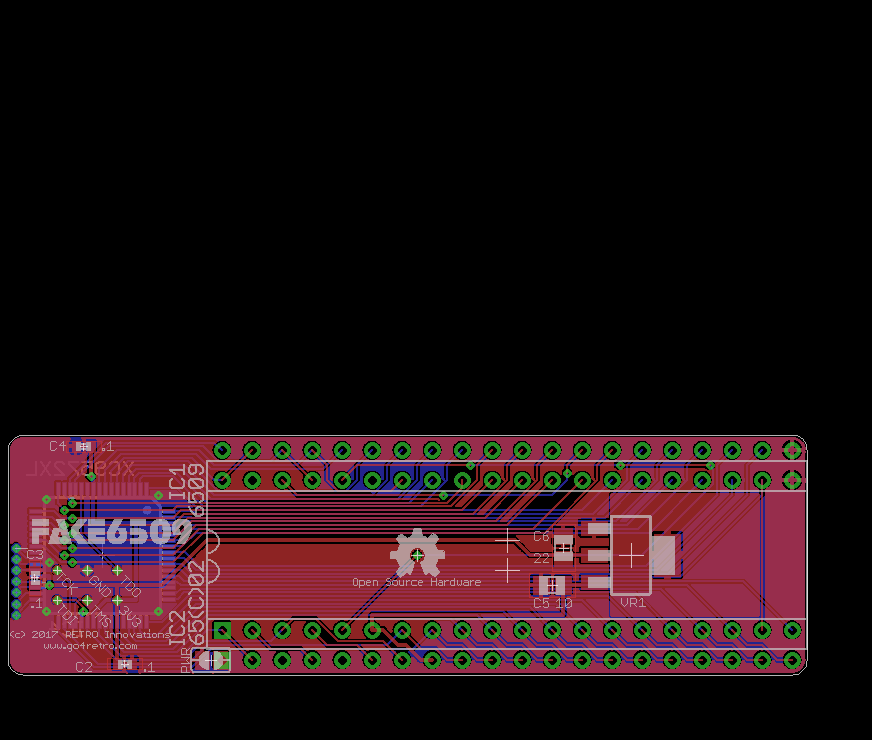
Sorry for resurrecting a long ago thread, but I created a PCB for a 6509 Replacement:


I am considering building a few test boards, if someone is interested in testing.
Jim


I am considering building a few test boards, if someone is interested in testing.
Jim
- BigDumbDinosaur
- Posts: 9428
- Joined: 28 May 2009
- Location: Midwestern USA (JB Pritzker’s dystopia)
- Contact:
Re: MOS 6509 look-alikes?
brain wrote:
Sorry for resurrecting a long ago thread, but I created a PCB for a 6509 Replacement:
...
I am considering building a few test boards, if someone is interested in testing.
Jim
...
I am considering building a few test boards, if someone is interested in testing.
Jim
x86? We ain't got no x86. We don't NEED no stinking x86!
Re: MOS 6509 look-alikes?
Thanks Jim, that's a very interesting development!
Re: MOS 6509 look-alikes?
Very nice! This is long overdue.
Steve
Steve
-
DerTrueForce
- Posts: 483
- Joined: 04 Jun 2016
- Location: Australia
Re: MOS 6509 look-alikes?
It's usually a good idea to post schematics in black and white, because there are some people here that are colour-blind.
Re: MOS 6509 look-alikes?
For reference and for interest, there's a long and active thread over on the cbm-hackers mailing list discussing "Hardware emulation of 6509 using 6502?" which are worth a read - hopefully as and when some excellent discoveries are made or conclusions reached we can summarise or link to them:
http://www.softwolves.com/arkiv/cbm-hac ... html#25459
http://www.softwolves.com/arkiv/cbm-hac ... html#26201
http://www.softwolves.com/arkiv/cbm-hac ... html#25459
http://www.softwolves.com/arkiv/cbm-hac ... html#26201
Re: MOS 6509 look-alikes?
BigEd wrote:
For reference and for interest, there's a long and active thread over on the cbm-hackers mailing list discussing "Hardware emulation of 6509 using 6502?" which are worth a read - hopefully as and when some excellent discoveries are made or conclusions reached we can summarise or link to them:
http://www.softwolves.com/arkiv/cbm-hac ... html#25459
http://www.softwolves.com/arkiv/cbm-hac ... html#26201
http://www.softwolves.com/arkiv/cbm-hac ... html#25459
http://www.softwolves.com/arkiv/cbm-hac ... html#26201
In short:
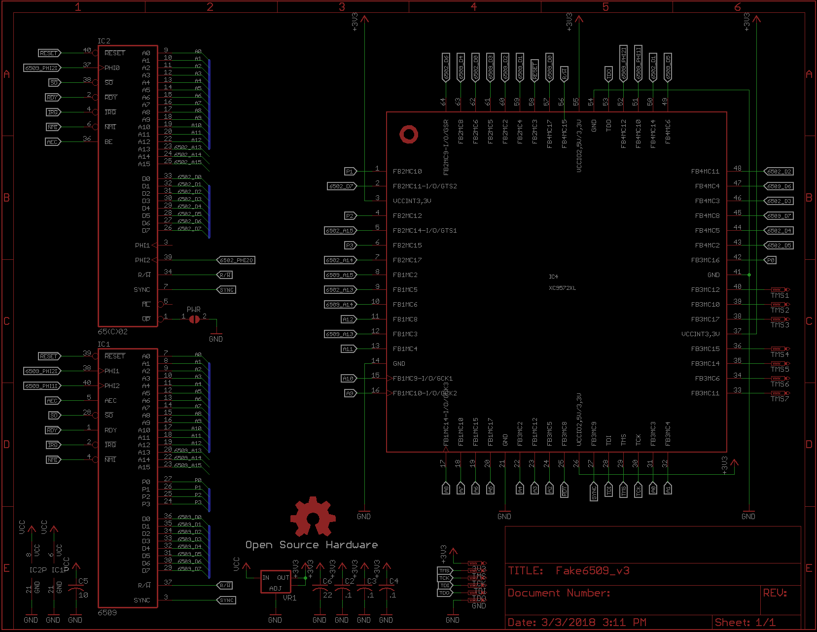
I implemented Dr. Jefyll's schematic from this thread in a small piggyback PCB.
We determined that the design also should trap the databus, so as to not read from the computer during a $0/$1 read (next design rev)
There are potential issues with the CLK signal (6509 uses external clocks, 6502 creates them internally)
Currently, we are tracking down a problem where a write on the 6502 does not push the right value to the databus (or, it does not keep it there long enough)
There's a companion thread to discover the specific nature of the indirect addressing (page crossings, behavior when writing value, etc.)
Jim
Re: MOS 6509 look-alikes?
All very interesting Jim, thanks for the update!
Re: MOS 6509 look-alikes?
brain wrote:
It's a shame the Interwebs have not found a way to "join" a discussion across two forums
If it's helpful at all, here's Jim's schematic again with new colors plus a note or two I added. This initial implementation connects the 65C02 data bus directly to the motherboard, but a future version will establish that connection via the CPLD so the 65C02 can when necessary listen to the CPLD only and not the motherboard, for the reason Jim noted.
In 1988 my 65C02 got six new registers and 44 new full-speed instructions!
https://laughtonelectronics.com/Arcana/ ... mmary.html
https://laughtonelectronics.com/Arcana/ ... mmary.html
Re: MOS 6509 look-alikes?
Astonishing update from Jim Brain! I'm still rubbing my eyes after reading the last line of this section. 
Quote:
Updates:
* After not having success with the '245 daughter-board, I wired up a 50MHz oscillator in hopes that I could synthesize a proper PHI_IN for the 6502 such that the PHI2_OUT would match the PHI2 on the PCB.
* After not having success, I started probing the R/W line, on the assumption that it was being forced to an incorrect state.
* I looked at the schematic, and I noticed U12, which appears to be a databus buffer for the RAM.
* I tapped pin 1 and looked at it.
* I then noticed that, aside from being inverted, it was occurring at the wrong half of the 6502 cycle.
o On the 6509, PHI2 goes low, R/W will go low for the upcoming write cycle, PHI2 goes high, '245 pin 1 goes high for a half cycle, and then goes low at the moment R/W goes high.
o On the 6502, PHI2 on the 6502 goes low, R/W will go low for the cycle to do the write, and immediately the pin 1 goes high, going low just as phi2 on the 6502 goes high
* On a hunch, I inverted the PHI signal going to the 6502, so it matched PHI1_6509.
The B128 booted up.
I had been using the following datasheet for the 6509 reference: http://archive.6502.org/datasheets/mos_6509_mpu.pdf
Which is linked from Wikipedia, and from the 6502.org web site.
which shows pin 40 as PHI2_IN, and pin 38 as PHI1_IN
But, the p500 schematics on Zimmers.net shows them reversed:
http://www.zimmers.net/anonftp/pub/cbm/ ... 01of15.gif
As does the B128 LP schematic:
http://www.zimmers.net/anonftp/pub/cbm/ ... 4-left.gif
And the B128 HP Schematic:
http://www.zimmers.net/anonftp/pub/cbm/ ... 059-01.gif
Thus, it appears the official datasheet is wrong, and has been wrong for 40 years.
<snip>
In 1988 my 65C02 got six new registers and 44 new full-speed instructions!
https://laughtonelectronics.com/Arcana/ ... mmary.html
https://laughtonelectronics.com/Arcana/ ... mmary.html
Re: MOS 6509 look-alikes?
Astonishing indeed. And that means that other sources, which presumably copied the datasheet, are wrong too, e.g. this one: http://mhv.bplaced.de/test/pinout/6509
Re: MOS 6509 look-alikes?
I assume all copies, everywhere are wrong.
The challenge is going to be how one fixes it. 6502.org stores the datasheet both as a working copy for folks to consult during repairs (and new efforts, such as this one), and for posterity. In this case, where such a fundamental error has been found, does 6502.org "fix" the posted and linked copy (storing the original elsewhere to maintain the archival qualities), or not?
The challenge is going to be how one fixes it. 6502.org stores the datasheet both as a working copy for folks to consult during repairs (and new efforts, such as this one), and for posterity. In this case, where such a fundamental error has been found, does 6502.org "fix" the posted and linked copy (storing the original elsewhere to maintain the archival qualities), or not?