Monster Decoding Logic

Re: Monster Decoding Logic
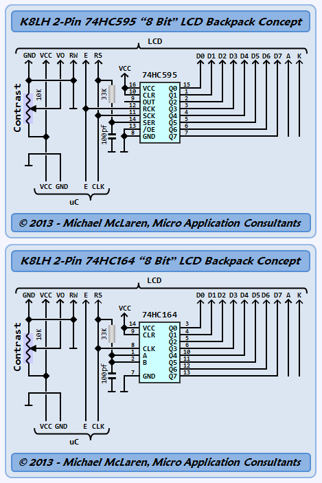
Is an LCD 'backpack' out of the question? Lots of possibilities (I2C, SPI, Serial, custom). Here's a design that drives the LCD in 8-bit interface mode while using a 2-pin interface to the host.
-
Alarm Siren

- Posts: 363
- Joined: 25 Oct 2016
Re: Monster Decoding Logic
Hmm. Yes, switching out to an SPI based interface would work, I've already got an SPI bus going on the board and I do have a spare SPI CS pin. Obviously it'd be slower than directly writing to the chip, but that is a possible solution certainly.
Want to design a PCB for your project? I strongly recommend KiCad. Its free, its multiplatform, and its easy to learn!
Also, I maintain KiCad libraries of Retro Computing and Arduino components you might find useful.
Also, I maintain KiCad libraries of Retro Computing and Arduino components you might find useful.
-
GARTHWILSON

- Forum Moderator
- Posts: 8773
- Joined: 30 Aug 2002
- Location: Southern California
- Contact:
Re: Monster Decoding Logic
Alarm Siren wrote:
GARTHWILSON wrote:
(at 5MHz) handles the LCD (plus five other things) through the first VIA
- LCD
- 5-key keypad
- beeper
- printer port
- T1 interrupts for software real-time clock, calendar, and alarms with 1/100th-second (10ms) resolution
- I²C port
- triggering the A/D convertor (which puts the data on another VIA)
- "Abort" button (like Reset but less drastic)
- and a synchronous serial port for things like my analog oscilloscope raster-graphics display
As for room, you can put other ICs under the VIA:
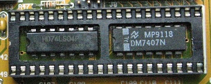
ICs under ICs are slightly visible in this photo also:
Similarly, you can also use the VIA's SR for tons of input bits:
or even both inputs and outputs on the same VIA SR, at the same time, using a 74xx126 section to stop the final 165's output when you're outputting to the 595's, to prevent contention.
It's all in the 6502 primer.
If I seem a little feisty, it's because a rather new tire with no apparent previous damage blew out on our son's van a few hours ago on the freeway and he fishtailed and rolled the van over and over. It's a total loss. Fortunately he's not hurt.
http://WilsonMinesCo.com/ lots of 6502 resources
The "second front page" is http://wilsonminesco.com/links.html .
What's an additional VIA among friends, anyhow?
The "second front page" is http://wilsonminesco.com/links.html .
What's an additional VIA among friends, anyhow?
-
Alarm Siren
- Posts: 363
- Joined: 25 Oct 2016
Re: Monster Decoding Logic
GARTHWILSON wrote:
I use a single VIA for:
[snip]
all at the same time.
[snip]
all at the same time.
GARTHWILSON wrote:
As for room, you can put other ICs under the VIA:
GARTHWILSON wrote:
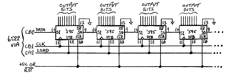
But really, for the amount of work you're going to put into it, the price of a second VIA is peanuts. Using the LCD in its 4-bit interface is easy, and probably won't be any less efficient than trying to manage it through other parallel logic which may slow your maximum clock speed down anyway, and certainly won't be as slow as doing it through SPI if you have to bit-bang it (although I do like SPI, even bit-banged!). Michael's idea using the '595 could be pulled off with the VIA's serial port, shifting at half the phase-2 rate without the processor having to bit-bang. In fact, I've done the following to get well over a hundred output bits from the VIA's SR (shift register):
[snip pic]
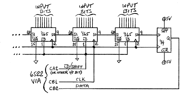
Similarly, you can also use the VIA's SR for tons of input bits:
[snip pic]
or even both inputs and outputs on the same VIA SR, at the same time, using a 74xx126 section to stop the final 165's output when you're outputting to the 595's, to prevent contention.
[snip pic]
Similarly, you can also use the VIA's SR for tons of input bits:
[snip pic]
or even both inputs and outputs on the same VIA SR, at the same time, using a 74xx126 section to stop the final 165's output when you're outputting to the 595's, to prevent contention.
I'm already using the VIA SR in exactly this manner to drive the keypad and status lights. I would rather not overload it with having to manage the screen as well.
GARTHWILSON wrote:
It's all in the 6502 primer.
GARTHWILSON wrote:
If I seem a little feisty, it's because a rather new tire with no apparent previous damage blew out on our son's van a few hours ago on the freeway and he fishtailed and rolled the van over and over. It's a total loss. Fortunately he's not hurt.
Want to design a PCB for your project? I strongly recommend KiCad. Its free, its multiplatform, and its easy to learn!
Also, I maintain KiCad libraries of Retro Computing and Arduino components you might find useful.
Also, I maintain KiCad libraries of Retro Computing and Arduino components you might find useful.
-
BigDumbDinosaur

- Posts: 9426
- Joined: 28 May 2009
- Location: Midwestern USA (JB Pritzker’s dystopia)
- Contact:
Re: Monster Decoding Logic
GARTHWILSON wrote:
If I seem a little feisty, it's because a rather new tire with no apparent previous damage blew out on our son's van a few hours ago on the freeway and he fishtailed and rolled the van over and over. It's a total loss. Fortunately he's not hurt.
x86? We ain't got no x86. We don't NEED no stinking x86!
Re: Monster Decoding Logic
There's been mention in the past of using a ROM or RAM chip for address decoding but I haven't seen it used. Could this be a viable decoder solution for lower speed systems? Could a 55-nS Parallel Flash chip decode fast enough for a 4-MHz system?
Cheerful regards, Mike
PS: Happy to hear your son is ok, Garth.
Cheerful regards, Mike
PS: Happy to hear your son is ok, Garth.
- Attachments
-
Last edited by Michael on Sun Oct 01, 2017 3:44 pm, edited 1 time in total.
-
Alarm Siren
- Posts: 363
- Joined: 25 Oct 2016
Re: Monster Decoding Logic
In that circuit, there's nothing to mask off the A14-A16 lines from the RAM when accessing the Standard RAM area. You'd need a multiplexer controlled by the decoder ROM, or perhaps sacrifice three of the I/O chip selects in order to "pass through" the A14-A16 lines when appropriate (there's some spare address inputs on the decoder ROM so it could be done). Also I've not come across ROM chips that are that quick, but I assume they must exist.
How are you making these diagrams? they're absolutely beautiful
How are you making these diagrams? they're absolutely beautiful
Want to design a PCB for your project? I strongly recommend KiCad. Its free, its multiplatform, and its easy to learn!
Also, I maintain KiCad libraries of Retro Computing and Arduino components you might find useful.
Also, I maintain KiCad libraries of Retro Computing and Arduino components you might find useful.
Re: Monster Decoding Logic
Sorry! The memory map insert was incorrect. That drawing is for your design with two RAM chips so the 128K RAM is only selected when the 6502 addresses the $8000-BFFF block.
* Drawings are from Microsoft Excel
* Drawings are from Microsoft Excel
- Attachments
-
Last edited by Michael on Sun Oct 01, 2017 6:12 pm, edited 1 time in total.
Re: Monster Decoding Logic
As you noted, supporting a single 128K RAM chip instead of two RAM chips would require giving up some of the decoder I/O chip select outputs...
- Attachments
-
Last edited by Michael on Mon Oct 02, 2017 5:05 pm, edited 2 times in total.
-
Alarm Siren
- Posts: 363
- Joined: 25 Oct 2016
Re: Monster Decoding Logic
Such decadance I have to try. Pray explain how Excel can be coaxed into making such images.
Want to design a PCB for your project? I strongly recommend KiCad. Its free, its multiplatform, and its easy to learn!
Also, I maintain KiCad libraries of Retro Computing and Arduino components you might find useful.
Also, I maintain KiCad libraries of Retro Computing and Arduino components you might find useful.
-
BigDumbDinosaur
- Posts: 9426
- Joined: 28 May 2009
- Location: Midwestern USA (JB Pritzker’s dystopia)
- Contact:
Re: Monster Decoding Logic
Alarm Siren wrote:
Also I've not come across ROM chips that are that quick, but I assume they must exist.
x86? We ain't got no x86. We don't NEED no stinking x86!
Re: Monster Decoding Logic
You can get 45ns, 5v flash from Microchip, provided you don't mind using PLCC parts.
Re: Monster Decoding Logic
Still fleshing out ideas. I wonder if anyone other than Jeff (Dr Jefyll) recognizes the bank select method in the crude design below?
reference: Ultra-fast output port using 65C02 illegal instructions
reference: Ultra-fast output port using 65C02 illegal instructions
- Attachments
-
Last edited by Michael on Thu Oct 05, 2017 11:33 pm, edited 2 times in total.
-
Alarm Siren
- Posts: 363
- Joined: 25 Oct 2016
Re: Monster Decoding Logic
I recognise it. I did very seriously consider using something like it, but I decided that it was important that the bank bits be readable as well as writable so that subroutines / interrupts can save and restore them. For your CLKGEN is that a PIC?
Want to design a PCB for your project? I strongly recommend KiCad. Its free, its multiplatform, and its easy to learn!
Also, I maintain KiCad libraries of Retro Computing and Arduino components you might find useful.
Also, I maintain KiCad libraries of Retro Computing and Arduino components you might find useful.