I haven't found any information on how to do this on this site, so I decided to do it myself.
http://kaput.homeunix.org/~thrashbarg/6502ss.jpg
This could easily be made into a small board and wired to the 6502 directly, as it only needs three pins, provided RDY is cut first (might be a bit tricky on a PCB).
Also, if you want to change the default state from whatever it is (stopped or running), disconnect the wire which goes between the 74LS00 B pin 4 to 74LS00 A pin 11 on the 74LS00 A side and attach it to 74LS00 A pin 8. Hope you understand that... The function of the RUN/STOP switch will be reversed too.
My web server's a tad dodgy (you can thank Bigpond for that) so it may not be available all the time.
Tell me what you think or if there are any problems!
Thrashbarg
Update: I've discovered a major bug with the design, it halts the 6502 AFTER the sync cycle, so you end up skipping an instruction on 1 byte commands or pointing to the first memory location on 2 or 3 byte commands. This is because SYNC goes high with phase-1 and there's a delay between the two on in the logic. I.e. The flip flop gets a clock cycle before the data is updated. I'll update the schematic if I find the solution.
Update: Got it working correctly now. I've updated the schematic. SYNC is run through the other half of the 74LS123 to give it a pulse, because it remians on during the halted period (I'm not using a MOS 6502, perhaps someone could test it on an original), and this causes the NAND flip flop to get confused. Also, rather than using another 74LS00 to debounce the RUN/STOP switch I attached it to the other half of the 74LS74, which brings the total chip count down to three. The RUN/STOP switch is synchronised with Phase-1 by the first half of the 74LS74, so there's no chance of RDY going low outside of the time specified by the datasheet.
6502 single step with 3 74LS chips
-
Thrashbarg
- Posts: 26
- Joined: 24 Nov 2004
- Location: Adelaide
- Contact:
6502 single step with 3 74LS chips
Last edited by Thrashbarg on Mon Jun 12, 2006 5:37 pm, edited 1 time in total.
Check out my 8080 project: http://kaput.homeunix.org

Re: 6502 single step with 4 74LS chips
Thrashbarg wrote:
I haven't found any information on how to do this on this site, so I decided to do it myself.
Code: Select all
    ___
   / __|__
  / /  |_/     Groetjes, Ruud
  \ \__|_\
   \___|       URL: www.baltissen.org
-
Thrashbarg
- Posts: 26
- Joined: 24 Nov 2004
- Location: Adelaide
- Contact:
That's an excellent debugger, but my idea is aimed towards someone who wants to wire it up on a bit of bread board quickly.
Sorry I didn't see it.
Sorry I didn't see it.
Check out my 8080 project: http://kaput.homeunix.org
Thrashbarg wrote:
Sorry I didn't see it.
Code: Select all
    ___
   / __|__
  / /  |_/     Groetjes, Ruud
  \ \__|_\
   \___|       URL: www.baltissen.org
-
Thrashbarg
- Posts: 26
- Joined: 24 Nov 2004
- Location: Adelaide
- Contact:
ah i see, sorry, I don't have any 74LS76's to play with 
Check out my 8080 project: http://kaput.homeunix.org
-
BitWise

- In Memoriam
- Posts: 996
- Joined: 02 Mar 2004
- Location: Berkshire, UK
- Contact:
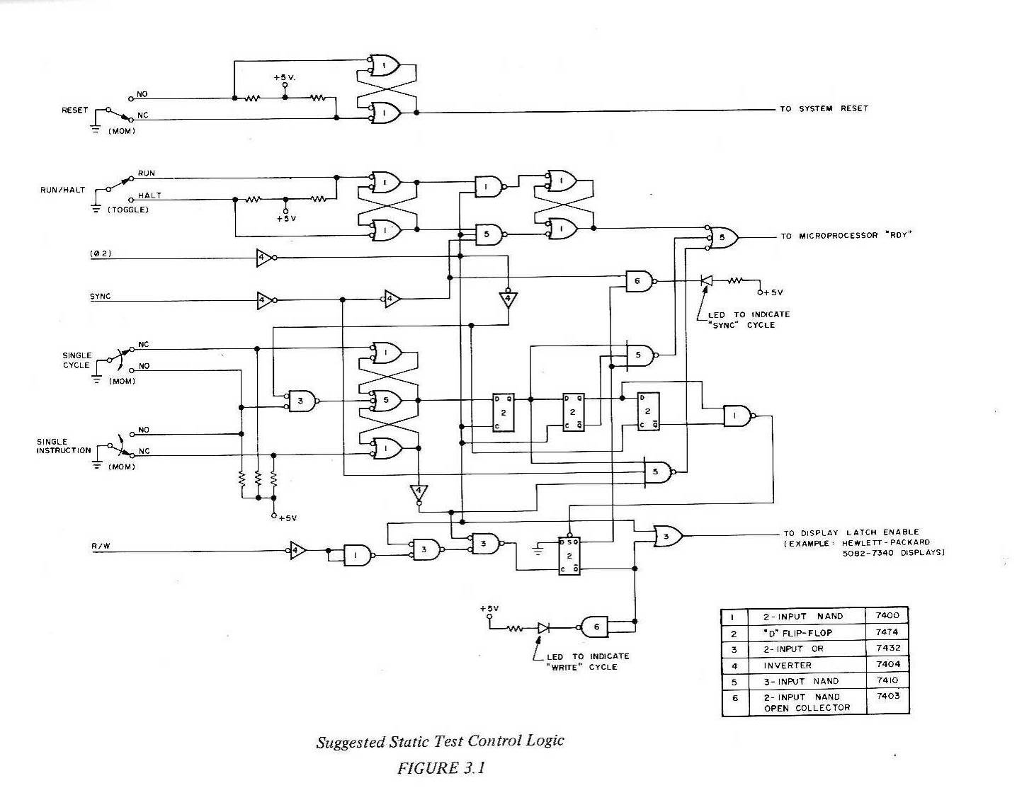
The MOS hardware manual for the 6502 contains the following circuit for static debugging.
Last edited by BitWise on Thu Jul 07, 2016 9:32 am, edited 1 time in total.
Andrew Jacobs
6502 & PIC Stuff - http://www.obelisk.me.uk/
Cross-Platform 6502/65C02/65816 Macro Assembler - http://www.obelisk.me.uk/dev65/
Open Source Projects - https://github.com/andrew-jacobs
6502 & PIC Stuff - http://www.obelisk.me.uk/
Cross-Platform 6502/65C02/65816 Macro Assembler - http://www.obelisk.me.uk/dev65/
Open Source Projects - https://github.com/andrew-jacobs
Thrashbarg wrote:
ah i see, sorry, I don't have any 74LS76's to play with ;)
Code: Select all
    ___
   / __|__
  / /  |_/     Groetjes, Ruud
  \ \__|_\
   \___|       URL: www.baltissen.org
-
Thrashbarg
- Posts: 26
- Joined: 24 Nov 2004
- Location: Adelaide
- Contact:
BitWise wrote:
The MOS hardware manual for the 6502 contains the following circuit for static debugging.
Check out my 8080 project: http://kaput.homeunix.org
Woz put a circuit for single step/single instruction using a single 7474 into the Apple 1 manual. Here's a link to the manual.
http://www.brielcomputers.com/files/a1man.pdf
Page 12 is what you are looking for. Ignore the slow ROM circuit. It works fine with my replica 1.
Vince
http://www.brielcomputers.com/files/a1man.pdf
Page 12 is what you are looking for. Ignore the slow ROM circuit. It works fine with my replica 1.
Vince
replica 1 the Apple 1 clone
http://www.brielcomputers.com
http://www.brielcomputers.com
-
BitWise
- In Memoriam
- Posts: 996
- Joined: 02 Mar 2004
- Location: Berkshire, UK
- Contact:
Have you tried stepping memory write intensive code with the Woz circuit?
The MOS manual advices not stopping a write cycle and thier circuit will skip to the next non-write cycle when stepping. Were they being overly cautious?
The MOS manual advices not stopping a write cycle and thier circuit will skip to the next non-write cycle when stepping. Were they being overly cautious?
Andrew Jacobs
6502 & PIC Stuff - http://www.obelisk.me.uk/
Cross-Platform 6502/65C02/65816 Macro Assembler - http://www.obelisk.me.uk/dev65/
Open Source Projects - https://github.com/andrew-jacobs
6502 & PIC Stuff - http://www.obelisk.me.uk/
Cross-Platform 6502/65C02/65816 Macro Assembler - http://www.obelisk.me.uk/dev65/
Open Source Projects - https://github.com/andrew-jacobs
I've mostly tried it with read cycles but I will try it with extensive writes to mem and see what the results are.
replica 1 the Apple 1 clone
http://www.brielcomputers.com
http://www.brielcomputers.com
-
BitWise
- In Memoriam
- Posts: 996
- Joined: 02 Mar 2004
- Location: Berkshire, UK
- Contact:
I've been playing around with trying to fit the single instruction/cycle logic on to a ATF16V8B PLD chip to be controlled by a PIC. (The cunning plan is to attach the PIC to the address bus, data bus and control lines so it can bootstrap the firmware into the SRAM before enabling the 6502 - It will then control the 65C02 and provide an RS-232 based debugger).
The CUPL looks like this
This generates the following signals:
When WDC deliver my order I can try it for real.
The CUPL looks like this
Code: Select all
Name        Debugger;
PartNo      NONE;
Date        16/08/2006;
Revision    01;
Designer    Andrew Jacobs;
Company     NONE;
Assembly    None;
Location    NONE;
Device      G16V8;


pin 1           = clk;

pin 2           = sync;

pin 4           = run;
pin 5           = step;
pin 6           = cycle;
pin 7           = !rst;

pin 12          = rdy;
pin 13          = stop;
pin 19          = !oe;

pin [14..16]    = [q2..0];

field state = [q2..0];

$define S0      'b'000
$define S1      'b'001
$define S2      'b'010
$define S3      'b'011
$define S4      'b'100
$define S5      'b'101
$define S6      'b'110
$define S7      'b'111

rdy     =   state:[S1,S2,S3,S5];
stop    =   state:[S0,S4,S6];

sequenced state {
/* S0 - STOPPED - No execution, waiting for a command */
present S0
    if      run & !step & !cycle    next S1;
    if     !run &  step & !cycle    next S3;
    if     !run & !step &  cycle    next S5;
    default next S0;

/* S1 - RUNNING - Processor is enabled until the run input is release */
present S1
    if      rst                     next S0;
    if     !rst & !run              next S2;
    default next S1;

/* S2 - RUNNING - The run signal is released, stop at the next sync */
present S2
    if      rst # sync              next S0;
    default next S2;

/* S3 - STEPPING - Enable processor until next sync */
present S3
    if      rst                     next S0;
    if     !rst & sync              next S4;
    default next S3;

/* S4 - STEPPING - Wait for step to be released */
present S4
    if      rst # !step             next S0;
    default next S4;

/* S5 - CYCLING - Enable processor for one cycle */
present S5
    if      rst                     next S0;
    default next    S6;

/* S6 - CYCLING - Wait for cycle to be release */
present S6
    if      rst # !cycle            next S0;
    default next S6;

/* S7 - Unused, force a reset */
present S7
    next S0;
}
6502.org wrote:
Image no longer available: http://www.obelisk.demon.co.uk/6502/traces.jpg
Andrew Jacobs
6502 & PIC Stuff - http://www.obelisk.me.uk/
Cross-Platform 6502/65C02/65816 Macro Assembler - http://www.obelisk.me.uk/dev65/
Open Source Projects - https://github.com/andrew-jacobs
6502 & PIC Stuff - http://www.obelisk.me.uk/
Cross-Platform 6502/65C02/65816 Macro Assembler - http://www.obelisk.me.uk/dev65/
Open Source Projects - https://github.com/andrew-jacobs
-
Mike Naberezny

- Site Admin
- Posts: 294
- Joined: 30 Aug 2002
- Location: Northern California
- Contact:
Re: 6502 single step with 3 74LS chips
Thrashbarg wrote:
Update: Got it working correctly now. I've updated the schematic. SYNC is run through the other half of the 74LS123 to give it a pulse, because it remians on during the halted period (I'm not using a MOS 6502, perhaps someone could test it on an original), and this causes the NAND flip flop to get confused. Also, rather than using another 74LS00 to debounce the RUN/STOP switch I attached it to the other half of the 74LS74, which brings the total chip count down to three. The RUN/STOP switch is synchronised with Phase-1 by the first half of the 74LS74, so there's no chance of RDY going low outside of the time specified by the datasheet.
Mike
- Mike Naberezny (mike@naberezny.com) http://6502.org
-
turfed-out
- Posts: 5
- Joined: 16 Apr 2009
single stepper
Hello Thrashbarg,
Is the single-stepper circuit for single instruction or single cycle stepping ?
Is the single-stepper circuit for single instruction or single cycle stepping ?
Re: 6502 single step with 3 74LS chips
I'm not sure if it's right for me to revive such an old thread, however I have built this circuit to try and debug my own 65c02 breadboard and thought it might help others who stumble across it.
I found the circuit does work as per Thrashbarg's schematic except I had to add ground connections to pins 6 & 14 of the 74ls123, as recommended in it's datasheet. Also because it relies on sync it's a single-stepper not a single cycle, but the run/stop switch can halt the CPU in the middle of an instruction. A subsequent step pulse then loads the next instruction. I used 470pf caps on the 74ls123 as I didn't have 330pf ones handy and it seems to be fine.
I found the circuit does work as per Thrashbarg's schematic except I had to add ground connections to pins 6 & 14 of the 74ls123, as recommended in it's datasheet. Also because it relies on sync it's a single-stepper not a single cycle, but the run/stop switch can halt the CPU in the middle of an instruction. A subsequent step pulse then loads the next instruction. I used 470pf caps on the 74ls123 as I didn't have 330pf ones handy and it seems to be fine.