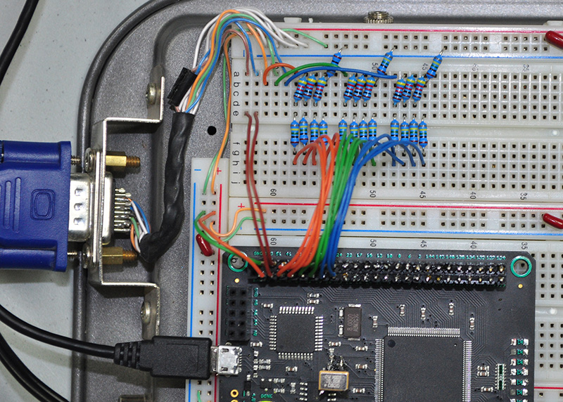
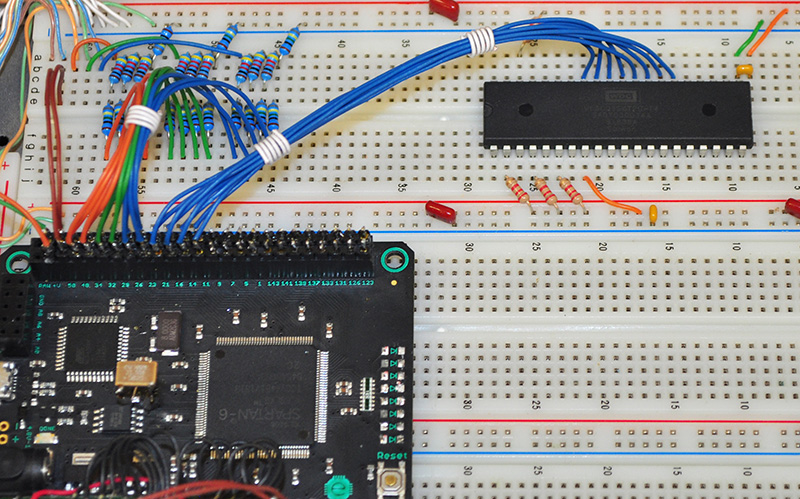
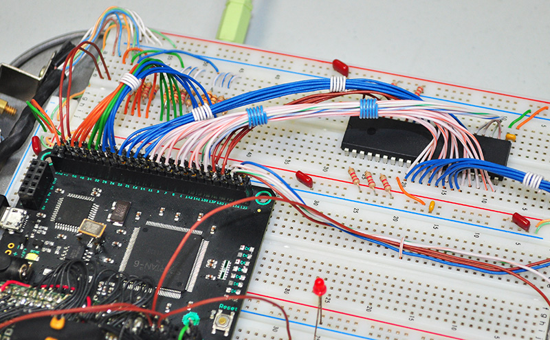
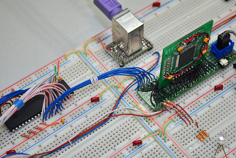
6502.org Forum  Projects  Code  Documents  Tools  Forum
It is currently Thu Nov 21, 2024 1:08 pm

All times are UTC


Post new topic Reply to topic  [ 83 posts ]  Go to page 1, 2, 3, 4, 5, 6  Next
Author Message
PostPosted: Fri Jun 16, 2017 6:06 pm 
Offline
User avatar

Joined: Mon May 25, 2015 2:25 pm
Posts: 690
Location: Gillies, Ontario, Canada
Greets to all 6502 Freaks!

I have decided to start a new lofty project I call “Anvil-6502”, or just A65 for short. There are several reasons for the name I have chosen…

1) The system uses a real 65C02 DIP, like my favorite computers of the 1980s.
2) The 6502 does all of the work, talking directly to the hardware (Bare Metal Model).
3) BMOS - The Operating System (Bare Metal Operating System) includes an assembler.

So, much like using an Anvil, you have to “Hit The Bare Metal” to write code for The A65!

Anvil-6502 will also be fully self-contained, and not rely on any outside input other than what is entered by the user on the attached keyboard. This is a fully working 6502 based computer that will include an IDE and several programming tools directly in the Operating System, which will all be running on the single onboard 65C02 Processor.

The reason for the existence of A65 is so that I can temporarily escape from the current world of bloated code, IP cores, code wizards, high level fluff, and “Duino” flavored spoon-feeding technologies that try to make it so that a stoned monkey could create a working program by randomly hammering on a keyboard, even if half the keys were broken. (whoa... I know!).

Another reason for A65 is so that my addiction to 6502 assembly programming can become portable. I do have other 6502 based projects on the go, but lately I have not had the time to sit relax in my basement lab and work on them. Since A65 will be about half the size of a C64, and simply plug into any standard VGA Monitor, Keyboard and Speaker System, I can move it around and use when I have some spare time.

This project is all about the 6502 and its assembly language. It is not about the supporting hardware that makes up what I call the “Chipset”. The Chipset will be whatever modern FPGA fits my design, which gives the 6502 some basic Graphics, Sound, and IO functionality.

So here are my “Must Have” Design Goals…

Code:
1)   The CPU will be a REAL 6502 in DIP Format.
2)   The system will boot with a functional Operating System.
3)   No reliance on modern equipment for coding.
4)   The OS will include an IDE and Assembler.
5)   Access to at least 4MB of Multimedia SRAM.
6)   Instant toggle between OS and assembled / running code.
7)   Decent Graphics and Sound built into the Chipset.
8)   Custom file system to use any mass storage device.
9)   Standard Monitor and Keyboard support.
10)   No ROMs. OS and Fonts sent to SRAM at boot.
11)   Small form factor case with 6502 behind backlit window.


Some expanded explanations of the design goals…

No reliance on modern equipment for coding means that all assembly will be entered, assembled, and run directly by A65. The OS will boot directly into the IDE, and allow assembling of the source code to another 64K segment in the 4MB address space. The OS segment will be protected from any access by the running program. All SRAM above the running program segment will be accessible by making function calls to the chipset. The running program can rewrite its own codespace, which will allow it to read code from extended memory and write it into the executable erea. This will allow the 6502 to essentially run a program of any size up to 4MB.

Right after an "Assemble and Execute" command is given by the OS, the chipset will grab the contents of Zero Page and store it internally until the OS is returned. A "Return to OS" command will be a keyboard hot key (ESC + F1). This way, the IDE can retain its state for things such as current source code scroll position, IDE settings, etc. Since the OS segment is protected from access by the running program, you can crash and burn all you like, and still return instantly to the OS, and then repair your code. This is what I consider old-school debugging ... just fix it and run it again until it works, man!

Source code will be stored as words in the remaining ~3MB of SRAM Data Space. The words will represent a color value and a character code. This will allow for approximately 32,000 lines of code to be worked on, each line having 64 characters of any color. I chose 64 characters since my VGA generator puts out a screen of 66x35 characters onto the 400x300 resolution display.

The 4MB of SRAM is to be divided into the following segments…

Code:
Video Buffer A : 0,000,000 (120K Protected)
Video Buffer B : 0,120,000 (120K Protected)
6502 Operating : 0,240,000 (64K Protected)
6502 Executable Program : 0,305,536 (64K Full Access)
Working Memory : 0,371,072 (up to 4 MB Total Memory)


As for Multimedia Capabilities, I am using the GPU design from previous work…

Code:
Video : VGA at 400 x 300 resolution with 256 colors from palette of 4096
Sound : 4 Independent 8 bit channels mixed down to 2 stereo channels
GPU : Transparent aware blitter and basic drawing functions
IO : PS2 keyboard, SD card slot, VGA port, audio port, USB (serial) port


The current FPGA GPU Core can move Sprites / Images at 20MHz bandwidth, which is more than enough to hurl a few hundred large sprites around at 60 frames per second. Sound is the same as an Amiga.

The goal is to do all code development right on the unit. I will also include some basic drawing programs and coding tools, which can be loaded as separate programs. A completed program will be stored on the external mass storage device, which at this point will probably be an SD card. I have detailed a file system that will allow the OS to include simple Load, Save and Delete commands.

In the case where I may want to “import” sound or graphics data from my PC into A65 for a demo or game, the onboard USB port can be used to stream bytes from the PC into A65. The USB port will be a simple FTDI USB to serial converter, and I will make a basic export program for the PC. This does not break my “no outside reliance” rule too badly, as it is only to import sound and graphics that have been converted. A65 will have the task of then saving these to the SD card using its own file system. There will be no ability to use the SD Card on a PC beside to backup images of SD cards for safe keeping.

The final cabinet will be around 10 inches wide by 6 inches deep, and have a sloped front as to show off the 6502 behind an LED backlit clear window. The color of the LED backlight will correspond to the mode of operation, such as OS running, Assembling, or Program Executing.

Ok, so there are my basic design goals and reasons for creating Anvil-6502.
Let the fun begin!

Cheers,
Radical Brad... never afraid to Hit The Bare Metal!

Last edited by Oneironaut on Sun Jun 18, 2017 3:56 pm, edited 7 times in total.

Top
 Profile  
Reply with quote  
PostPosted: Fri Jun 16, 2017 6:41 pm 
Offline
User avatar

Joined: Thu May 28, 2009 9:46 pm
Posts: 8503
Location: Midwestern USA
Oneironaut wrote:
[b]1) The system uses a real 65C02 DIP, like my favorite computers of the 1980s.

Why not use the 65C816?

_________________
x86?  We ain't got no x86.  We don't NEED no stinking x86!


Top
 Profile  
Reply with quote  
PostPosted: Fri Jun 16, 2017 6:49 pm 
Offline
User avatar

Joined: Fri Aug 30, 2002 1:09 am
Posts: 8543
Location: Southern California
I like the independence goal. Most jelly-bean SBCs out there rely on plugging in to a PC for development, and may require the supplier's software, or a particular OS, etc..

_________________
http://WilsonMinesCo.com/ lots of 6502 resources
The "second front page" is http://wilsonminesco.com/links.html .
What's an additional VIA among friends, anyhow?


Top
 Profile  
Reply with quote  
PostPosted: Fri Jun 16, 2017 7:40 pm 
Offline
User avatar

Joined: Mon May 25, 2015 2:25 pm
Posts: 690
Location: Gillies, Ontario, Canada
Thanks.

The 816 seems to "new" to me.
I started hacking on my PET 4016, and then moved on to the VIC-20, and C64.
A lot of this project is about reliving my past.
The days when I liked computers.

It all came apart for me after the Amiga500.
Upgrade, upgrade, replace, upgrade, reload, etc.
I currently get zero joy from a modern PC, since it runs me for the most part.

Remember the days when you clicked on your computer and it flashed right on up, ready to take your commands?
That was a good time in my life. I was still new enough to think that the hardware would remain the same forever, so I was able to really dig in and learn how to talk to the 6502 in the box.
Now you can throw out your obsolete PC in the same box it came in, since you just put the box in the attic a few months earlier!

So A65 is all about the 6502 and nothing else.
This is why I am placing the 6502 in a back-lit display window on the final product.

One day if 15 pin VGA really does vanish, I will just redo my chipset for HDMI or whatever flavor of the month is the accepted PC display standard by the latest graduates that rule the world with their ever changing and competing "standards". Same goes for the keyboard and mass storage device. What I do plan to keep the same is the final OS / IDE design and the actual multimedia specifications / commands.

When Anvil-6502 is completed, I intend to use it for the rest of my life, which should be a fair amount of time unless one of my high voltage experiments goes awry!

So for that reason, an 816 is as far from my mind as a Z80 or 8088.
Oh, and I still have both the fully functional PET and Vic-20!

Brad


Top
 Profile  
Reply with quote  
PostPosted: Fri Jun 16, 2017 9:21 pm 
Offline
User avatar

Joined: Thu May 28, 2009 9:46 pm
Posts: 8503
Location: Midwestern USA
GARTHWILSON wrote:
I like the independence goal. Most jelly-bean SBCs out there rely on plugging in to a PC for development, and may require the supplier's software, or a particular OS, etc..

I'd like to get POC to that point, but have been concentrating so far on hardware and basic firmware development. While I'm sure POC V2 has more than enough computing power and mass storage to support a software development environment, I'd have to write that environment, which would represent a major programming project in itself. So for the time being, I will continue to cross-develop.

_________________
x86?  We ain't got no x86.  We don't NEED no stinking x86!


Top
 Profile  
Reply with quote  
PostPosted: Fri Jun 16, 2017 9:26 pm 
Offline
User avatar

Joined: Thu May 28, 2009 9:46 pm
Posts: 8503
Location: Midwestern USA
Oneironaut wrote:
The 816 seems to "new" to me...So for that reason, an 816 is as far from my mind as a Z80 or 8088.

Well, I wouldn't put the '816 in the same category as those other MPUS. :shock: As for age, the '816 is (depending on whose timeline you believe) either 33 or 34 years old. Dunno about you, but I don't consider that "new." :? :D

As for the high voltage experiments...I'm shocked to think one of them might be charged with doing you in. :D

Good luck with your project.

_________________
x86?  We ain't got no x86.  We don't NEED no stinking x86!


Top
 Profile  
Reply with quote  
PostPosted: Sat Jun 17, 2017 1:43 am 
Offline
User avatar

Joined: Tue Mar 15, 2016 4:06 pm
Posts: 35
Will this one go on a PCB?

_________________
My 6502 Game System: https://hackaday.io/project/9325-dodo-6502-homebrew-game-system


Top
 Profile  
Reply with quote  
PostPosted: Sat Jun 17, 2017 3:24 am 
Offline

Joined: Sat Jun 04, 2016 10:22 pm
Posts: 483
Location: Australia
pnoyes: I think it'll have to. I can't imagine a solderless breadboard being very portable while it's built up.

I had a similar sort of idea to A65, inspired by Ben Heck's BASIC pocket computer. It looks suspiciously like mine won't end up fitting into my pockets, but it will be portable and self-contained. I won't say more about it here, because this is not my thread.


Top
 Profile  
Reply with quote  
PostPosted: Sat Jun 17, 2017 5:03 am 
Offline
User avatar

Joined: Mon May 25, 2015 2:25 pm
Posts: 690
Location: Gillies, Ontario, Canada
Thanks for the comments.

Yes, this unit will be destined for a real PCB, as well as a 3D printed cabinet, made from my SolidWorks model.
I will however, be making V1 on a breadboard to make sure my design goals can be met.
For this task, I dug up my "tiny" breadboard, which has been collecting dust since I made my larger ones.

Here is what I have done so far...

Image
An FPGA board with a Spartan-6 will be become the "Chipset".

I will eventually move to an Artix-7 FPGA, but for now will work around the slower Spartan-6.
By doing V1 using lesser parts and as more of a "hack", V2 will be guaranteed to work!

For now, I just slapped down two 512K 10ns SRAMS, but will eventually add eight so I have 4MB in total.
Fast SRAM is important since my bus sharing system will be intense, sharing the memory with...

1) The 6502 - gets access to all non protected SRAM whenever the GPU is not using it.
2) The GPU - gets exclusive access whenever a graphics command is issued by the 6502.
3) The Sound System - grabs 4 bytes on each horizontal line for its 4 voices.
4) The VGA Generator - Reads a line of 400 pixels @ 40 MHz so it can send them later at a slower rate.

If you thought the bus sharing and timing in a C128 was hairy, just wait until I detail this beast.
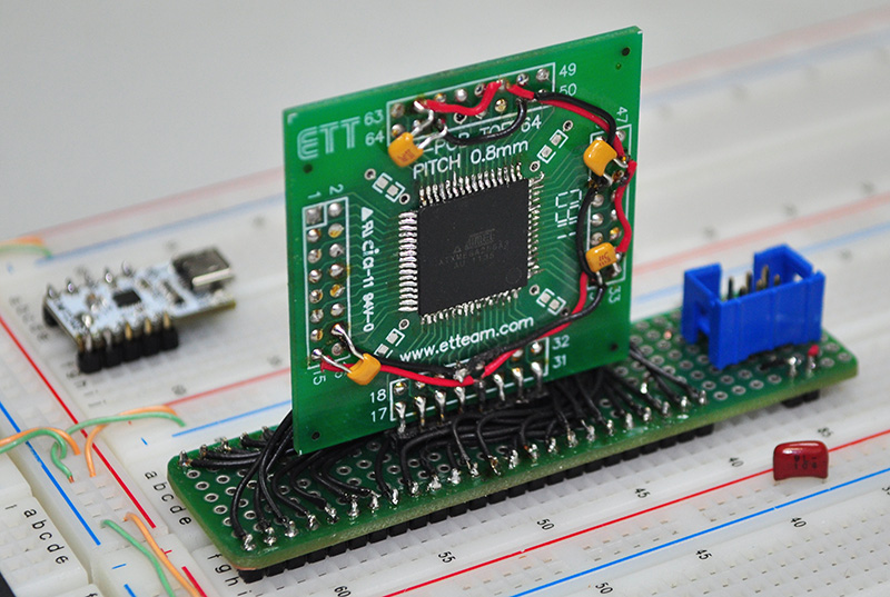
The bus arbiter inside A65 will be like an 8 bit digital orgy!

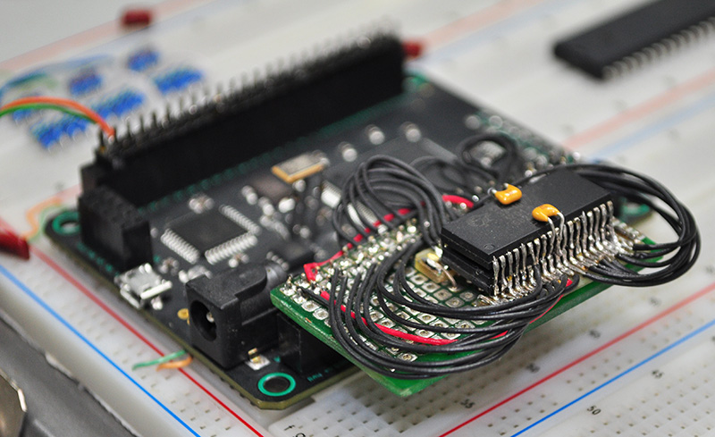
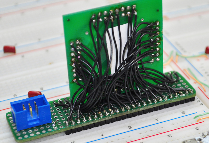
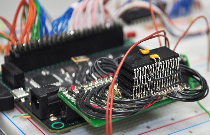
Here is the SRAM wired to the carrier board. Did I mention that V1 is a total hack job?...

Image
1 MB of fast SRAM, soon to become 4MB using 8 ICs instead of 2.

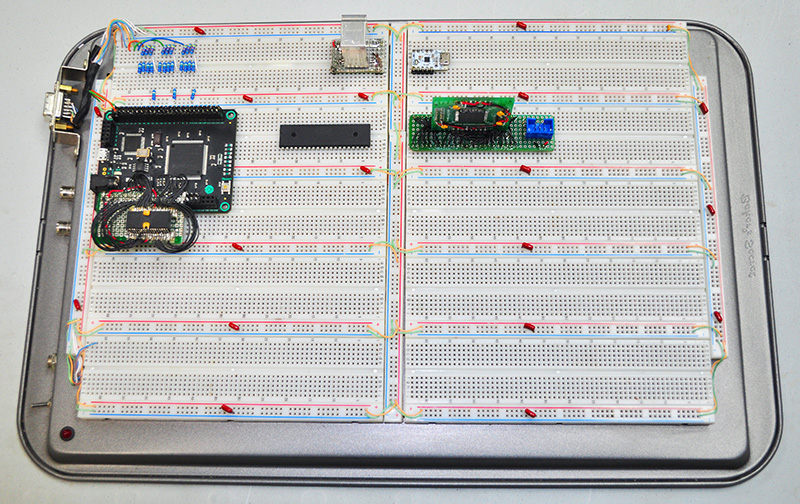
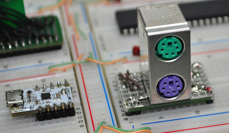
Here are the separate components that will make this system work.
Wow, this breadboard looks so tiny compared to my other MOABBs....

Image
The different components that will make up Anvil-6502.

Starting from the top left, the components on the board are as follows...

1) R2R resistor DAC to generate 4096 colors using a RRRR-GGGG-BBBB color space.
2) A PS2 keyboard port ripped from a mainboard I found at the local dump.
3) An FTDI USB to serial DIP board that will allow importing and backing up internal data.
4) The MOJO-V3 FPGA board that will host my Verilog GPU code.
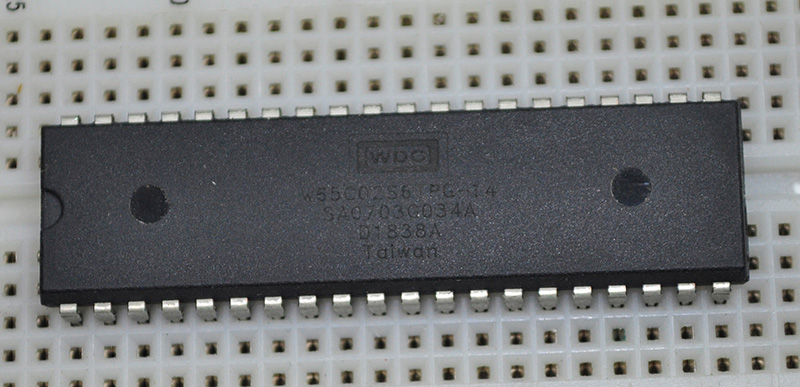
5) The one and only 65C02, as delivered from the Western Design Center.
6) An AVR that will talk to the mass storage device (probably an SD card).

I will start soldering up wires as soon as the rain drives me indoors for a few hours.
Since coding a complete GPU in HDL is as easy as chewing bubble gum, I expect to have A65 displaying something useful in a few days.
... all-righty-then!

Actually, because of my seriously limited free time, I will do most of the Verilog coding in notepad on my lunch hour, and then synthesize it for testing in the evening.
HDL is a funny beast to tame... some days you can make leaps and bounds effortlessly, and other days you fight what should be ultra simple. It is amazing amounts of fun!

Image

Talk at ya later,
Radical Brad


Top
 Profile  
Reply with quote  
PostPosted: Sat Jun 17, 2017 4:14 pm 
Offline
User avatar

Joined: Mon May 25, 2015 2:25 pm
Posts: 690
Location: Gillies, Ontario, Canada
Since there is not much to this hardware, it will come together quickly.
Most of the key components I already have mounted to carrier boards the fit the breadboard, so it will be just a matter of wiring them together. The real work will be in creating the HDL for the GPU, and then making all of the external systems talk to each other at high speed.

The MOJO board came with a 50MHz oscillator, but I prefer a 20MHz for VGA applications.
Using the PLL is easier this way, as there are no divisions, just clock multipliers.
In this case, I am going to start with 20MHz X 2 for a 40 MHz main clock.
Once things are working, I will try 20MHz x 3 for 60 MHz, but that may be too fast.
The external SRAM is 10ns, but considering setup and hold for a 2 way trip, 60MHz may not work.

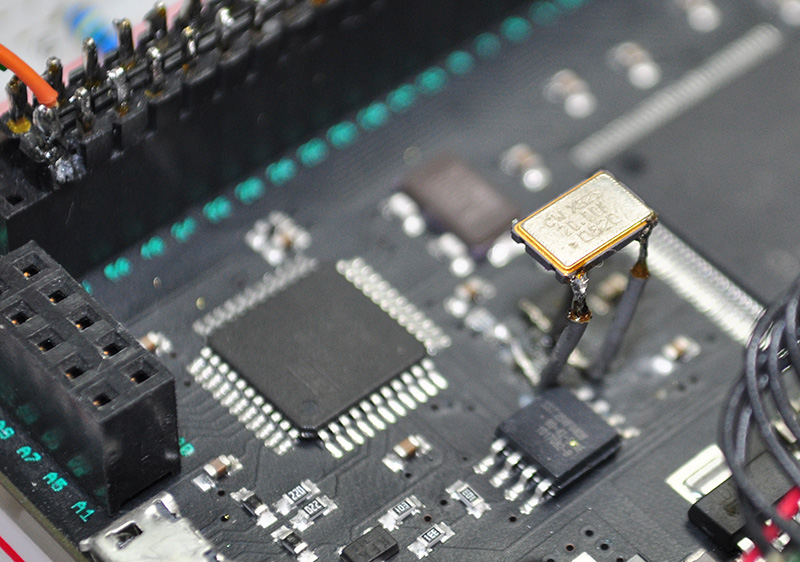
Another ugly hack. Ocsilator standing on wires after I razored off the traces...

Image
The FPGA oscillator is now 20Mhz

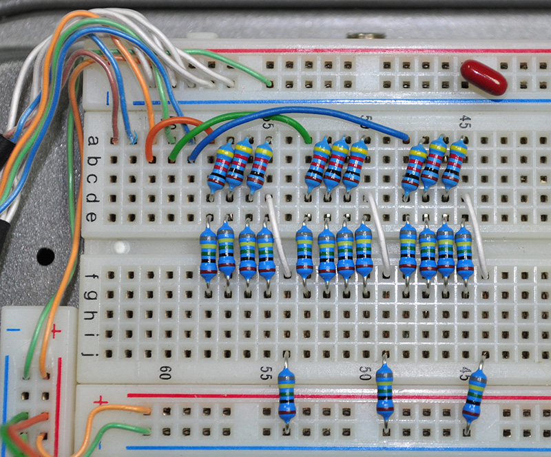
Threw a 12 bit DAC together as well...

Image
Each of the 4 bit segments can generate up to .75 volts.

Each of the primary colors has 4 bits, so I can have 16 shades of 16 colors for a uniform palette.
A65 will have a fully programmable palette as well so I can create any 256 of 4096 possible colors.
This will allow of color cycling effects and demo effects like plasma.


In order to load up the 6502 during development, I am using my DIP adapted Atmel Xmega-384...

Image
This is my rapid development superstar - 384K with a programming plug.

This uC is way overkill, but it does have 384K of program memory, so I am using it as a fake SD card right now.
To develop my OS and IDE, I will code on my PC using the great Kowalski Assembler, then load the through the AVR to the 6502.
Once the IDE and OS are working, they will be pre-loaded to the 6502 SRAM at power up by the FPGA.

In the completed design, the AVR will only have the task of streaming bits from the SD card to the 6502 OS.
At that point, I will choose a very small AVR, as I only need 10 IO between the FPGA and AVR.

You can also see the USB to serial adapter board in the background.
This will allow importing of assets such as sound data or graphics data from a PC.
Backing up of 6502 created SD cards to a PC for sharing will also be possible.
... that function assumes someone else may build one of these if I produce boards!

That's all for now.
The rain is breaking again, and I have 6 more raised beds to fill with dirt today.
I am doing this build during "breaks", which are usually limited to weather or my sore back!

Later,
Radical Brad


Top
 Profile  
Reply with quote  
PostPosted: Sun Jun 18, 2017 1:52 am 
Offline
User avatar

Joined: Mon May 25, 2015 2:25 pm
Posts: 690
Location: Gillies, Ontario, Canada
Wow, it only rained torrentially twice this afternoon and there was no hail or funnel clouds.
... probably means there will be two tomorrow!

Having done all my yard work today, gave me a bit of time to work some more on A65.

Here is the spaghetti side of my ultimate breadboard AVR...

Image
48 IO lines and a programming port.

I made this thing because I am always needing to load SRAMs with data, mostly on 6502 projects.
I can cram about 383K of data into the XMega, and it can stream this to any SRAM and then hide.
Right now it is holding the code for what will become my A65 OS, called BMOS... Bare Metal Operating System.

I have a PC program that takes the Kowalski Assembler output and then sends it to the XMEGA.
Its cool to be able to code up some 6502 assembly, and see it run within 10 seconds on the 6502!

Image
All incoming code will come from the operators keyboard.

Here is my PS2 port and the USB to serial chip that will deal with all IO.
I am only using a single PS2 port, as I have no use for a mouse in A65.
... real programmers type in their code and don't need to click ****!

Here is the guest of honor...

Image
65C02 as made by The Western Design Center.

Normally, I overclock EVERYTHING, even if it isn't necessary, but not this time.
I will run the 6502 at 8Mhz, which is well within the legal limit.
I have developed an interesting clocking scheme to allow optimum 6502 performance and memory sharing.
Here is the a small slice of my FPGA code that hands out the 6502 clock...

Code:
///////////////////////////////////////////////////////////////////////////////////////////////////////////////////////////////////////////////////////////////////
////////// 6502 CLOCK PHASE GENERATOR
///////////////////////////////////////////////////////////////////////////////////////////////////////////////////////////////////////////////////////////////////

// PHASE 1 OF 5 : WAIT FOR MEMORY ACCESS
if (BOOTSTEP == 255 & CKDIV == 0 & COMSTEP == 0 & MEMREADY == 1) begin
SRAMWE <= 1;
SRAMOE <= 1;
CPUBE <= 1;
CKDIV <= 1;
CPUCK <= 0;
end

// PHASE 2 OF 5 : NEXT CYCLE
if (CKDIV == 1) begin
CKDIV <= 2;
CPUCK <= 0;
end

// PHASE 2 OF 5 : SEND SRAM ADDRESS
if (CKDIV == 2) begin
CKDIV <= 3;
CPUCK <= 1;
end
if (CKDIV == 2 & (CPUADR < 512 | CPUADR > 767) & CPURW == 1) begin
MEMADR <= (CPUADR + CPUPAGE);
SRAMOE <= 0;
end

// PHASE 3  OF 5 : NEXT CYCLE
if (CKDIV == 3) begin
SRAMOE <= 1;
CKDIV <= 4;
CPUCK <= 1;
end

// PHASE 4 OF 5 : WRITE TO SRAM
if (CKDIV == 3 & (CPUADR < 512 | CPUADR > 767) & CPURW == 0) begin
MEMADR <= (CPUADR + CPUPAGE);
SRAMSEND <= CPUDAT;
SRAMWE <= 0;
end

// PHASE 4 OF 5 : WRITE TO COMMAND FROM 512 TO 749
if (CKDIV == 3 & CPUADR > 511 & CPUADR < 750 & CPURW == 0) begin
COMMAND <= CPUADR;
COMDATA <= CPUDAT;
COMSTEP <= 1;
CKDIV <= 0;
end

// PHASE 4 OF 5 : READ FROM SRAM OR COMMAND FROM 750 TO 767
if (CKDIV == 3 & (CPUADR < 512 | CPUADR > 749) & CPURW == 1) begin
CPUSEND <= SRAMDAT;
SRAMOE <= 1;
end

// PHASE 5 OF 5 : CLOSE SRAM
if (CKDIV == 4) begin
CPUBE <= 0;
CKDIV <= 0;
CPUCK <= 1;
end


It probably makes no sense to anyone other than me!
I find with HDL, you pretty much need to be the author in order to make total sense of code.
It basically sets an IO space right after the hardward stack of 256 bytes.
This IO space is interpreted by the FPGA as commands or requests for data.

I also rip the 6502 off the bus after the last clock slice so that the GPU can decide when memory is safe again.
Since the VGA generator is king, GPU commands, sound commands, and the 6502 are told when they can use SRAM.
There is a bus sharing hierarchy going on that works very well, and it took my some time to get it all working!

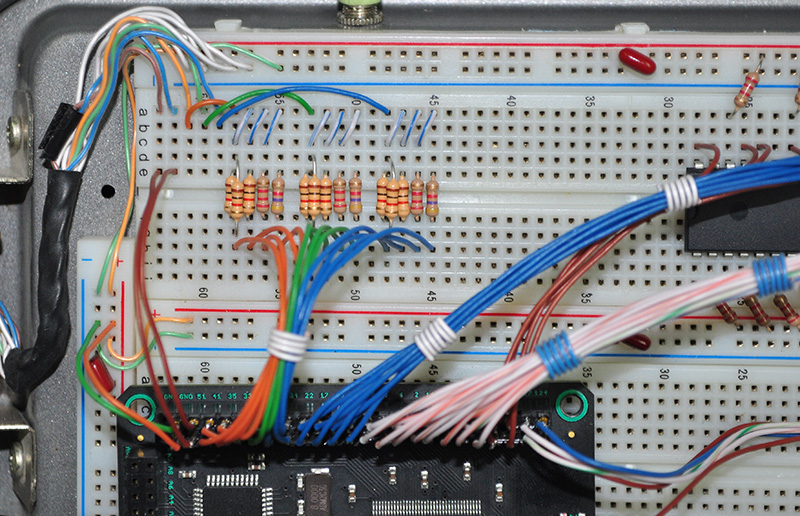
Finally, things are starting to look real, as wires get soldered onto the header pins...

Image
The VGA port is now wired to the board.

The wiring above is all that is required to drive any VGA monitor.
Horizontal Sync, Vertical Sync, and the Color Bits.

I am reworking the VGA generator from my Fusion-6502 project, so I already know it works.
VGA is drawn as 400x300 pixels over an 800x600 VGA standard screen by dividing by two.
The generator can also do 800x600, but that is just too much screen for a retro system.

Look who came to the party...

Image
The 65C02 gets jacked into the Matrix.

Normally, I develop everything first and then drop in the 6502, but this time I am doing it the other way.
Since the FPGA will take commands from the 6502, I need code running on the 6502 right away.
There will be no help from the AVR of FPGA when it comes to the OS... the 6502 is driving the bus!

I still have some address lines, and the data transfer lines from the AVR to connect, but that's about it.
6502 code will be up and running as soon as I get the FPGA boot sequence and SRAM stuffing code done.

I look forward to having a 6502 based computer again.
The fact that it will be off the modern grid is going to be great.
Just a flashing cursor and whatever code I enter.

...See you soon good ole' days!

Radical Brad


Top
 Profile  
Reply with quote  
PostPosted: Sun Jun 18, 2017 4:57 pm 
Offline
User avatar

Joined: Mon May 25, 2015 2:25 pm
Posts: 690
Location: Gillies, Ontario, Canada
Scattered showers so far this morning, I I managed to get some soldering time in.

Since everything hinges on having the 6502 up and running, I completed the adress bus and control line...

Image
The 6502 is now fully connected to the Chipset.

This nice thing about FPGA design is that an IO pin is nothing until you define it.
For the most part, you just connect wires and then tell a pin what it is anywhere on the device.
A65 will use almost all of the IO on the Spartan6 144 pin device, so I won't need a BGA package this time.

Here is the 6502 part of my "UCF File", which is the file that tells the FPGA what IO pins do what....

Code:
########################################################################################################################
########## EXTERNAL CPU PORT
########################################################################################################################

net CPUDAT[0]  loc = P21  | IOSTANDARD = LVTTL | DRIVE = 24 | SLEW = FAST | IOB = TRUE; # 6502 PIN 33
net CPUDAT[1]  loc = P22  | IOSTANDARD = LVTTL | DRIVE = 24 | SLEW = FAST | IOB = TRUE; # 6502 PIN 32 
net CPUDAT[2]  loc = P16  | IOSTANDARD = LVTTL | DRIVE = 24 | SLEW = FAST | IOB = TRUE; # 6502 PIN 31 
net CPUDAT[3]  loc = P17  | IOSTANDARD = LVTTL | DRIVE = 24 | SLEW = FAST | IOB = TRUE; # 6502 PIN 30
net CPUDAT[4]  loc = P14  | IOSTANDARD = LVTTL | DRIVE = 24 | SLEW = FAST | IOB = TRUE; # 6502 PIN 29
net CPUDAT[5]  loc = P15  | IOSTANDARD = LVTTL | DRIVE = 24 | SLEW = FAST | IOB = TRUE; # 6502 PIN 28
net CPUDAT[6]  loc = P11  | IOSTANDARD = LVTTL | DRIVE = 24 | SLEW = FAST | IOB = TRUE; # 6502 PIN 27
net CPUDAT[7]  loc = P12  | IOSTANDARD = LVTTL | DRIVE = 24 | SLEW = FAST | IOB = TRUE; # 6502 PIN 26
net CPUADR[0]  loc = P9   | IOSTANDARD = LVTTL | DRIVE = 24 | SLEW = FAST | IOB = TRUE; # 6502 PIN 09
net CPUADR[1]  loc = P10  | IOSTANDARD = LVTTL | DRIVE = 24 | SLEW = FAST | IOB = TRUE; # 6502 PIN 10
net CPUADR[2]  loc = P7   | IOSTANDARD = LVTTL | DRIVE = 24 | SLEW = FAST | IOB = TRUE; # 6502 PIN 11
net CPUADR[3]  loc = P8   | IOSTANDARD = LVTTL | DRIVE = 24 | SLEW = FAST | IOB = TRUE; # 6502 PIN 12
net CPUADR[4]  loc = P5   | IOSTANDARD = LVTTL | DRIVE = 24 | SLEW = FAST | IOB = TRUE; # 6502 PIN 13
net CPUADR[5]  loc = P6   | IOSTANDARD = LVTTL | DRIVE = 24 | SLEW = FAST | IOB = TRUE; # 6502 PIN 14
net CPUADR[6]  loc = P1   | IOSTANDARD = LVTTL | DRIVE = 24 | SLEW = FAST | IOB = TRUE; # 6502 PIN 15
net CPUADR[7]  loc = P2   | IOSTANDARD = LVTTL | DRIVE = 24 | SLEW = FAST | IOB = TRUE; # 6502 PIN 16
net CPUADR[8]  loc = P143 | IOSTANDARD = LVTTL | DRIVE = 24 | SLEW = FAST | IOB = TRUE; # 6502 PIN 17
net CPUADR[9]  loc = P144 | IOSTANDARD = LVTTL | DRIVE = 24 | SLEW = FAST | IOB = TRUE; # 6502 PIN 18
net CPUADR[10] loc = P141 | IOSTANDARD = LVTTL | DRIVE = 24 | SLEW = FAST | IOB = TRUE; # 6502 PIN 19
net CPUADR[11] loc = P142 | IOSTANDARD = LVTTL | DRIVE = 24 | SLEW = FAST | IOB = TRUE; # 6502 PIN 20
net CPUADR[12] loc = P139 | IOSTANDARD = LVTTL | DRIVE = 24 | SLEW = FAST | IOB = TRUE; # 6502 PIN 22
net CPUADR[13] loc = P140 | IOSTANDARD = LVTTL | DRIVE = 24 | SLEW = FAST | IOB = TRUE; # 6502 PIN 23
net CPUADR[14] loc = P137 | IOSTANDARD = LVTTL | DRIVE = 24 | SLEW = FAST | IOB = TRUE; # 6502 PIN 24
net CPUADR[15] loc = P138 | IOSTANDARD = LVTTL | DRIVE = 24 | SLEW = FAST | IOB = TRUE; # 6502 PIN 25
net CPURW        loc = P133 | IOSTANDARD = LVTTL | DRIVE = 24 | SLEW = FAST | IOB = TRUE; # 6502 PIN 34
net CPUCK        loc = P134 | IOSTANDARD = LVTTL | DRIVE = 24 | SLEW = FAST | IOB = TRUE; # 6502 PIN 37
net CPURS        loc = P131 | IOSTANDARD = LVTTL | DRIVE = 24 | SLEW = FAST | IOB = TRUE; # 6502 PIN 40
net CPUBE         loc = P132 | IOSTANDARD = LVTTL | DRIVE = 24 | SLEW = FAST | IOB = TRUE; # 6502 PIN 36


You can see that I filly control the address and data bus, as well as RWB, PHI2, RS, and BE.
All the other 6502 control pins are either tied high, low, or left unconnected as per the datasheet.

The other blue lines going from the low address bits to the AVR are for transferring OS code to SRAM on power up.
On initial power up, the FPGA holds the 6502 off the bus so it can sneak in and fill the SRAM with the operating system (BMOS).
After the 64k are written to the SRAM, the 6502 "page" is set there, and it is allowed to boot up into the OS.

After that, the AVR will only ever used again to send bytes from the mass storage device, probably an SD card.
I plan to make some basic command like "Set Storage Address", and "Read Byte at Address" type of thing.
The 6502 OS will have the task of turning storage data into a file structure of some kind.
The SD card will be read and written RAW as to further isolate A65 from the modern world.
We don't need no stinkin' FAT filesystem... yhe whole point of A65 is to be on a diet from all this modern bloat!

The AVR can transfer one byte at a time to the 6502 low address bus at while it is off the bus...

Image
Inter chip communication happens on address bits 0-7.

I also noticed that a used my 5 volt DAC design, which runs too "cold" for 3.3 volt operation.
I find that the best voltage for analog vga is fomr 0 to .75 volts, just a bit more than the spec.

I adjusted the resistors to get the proper voltage at 3.3v operation...

Image
The new RRRR-GGGG-BBBB DAC is much closer to the analog spec.

Since I had the soldering iron hot, I decided to stack on 2 more SRAMs so I have 2MB to work with.
A65 will eventually have 4MB, but 2MB is more than enough to test everything out.
The 3-8 multiplexer is made in the FPGA, so no external IC is required, just one line of simple code.

512K SRAM stacked 4 high makes 2MB of 8 bit memory...

Image
Parallel memory with their CE lines running to the FPGA

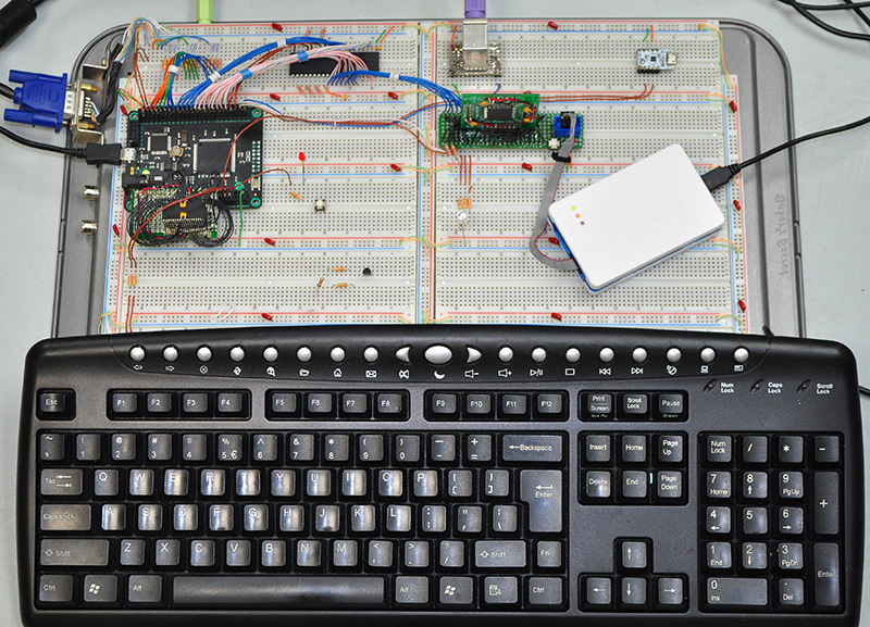
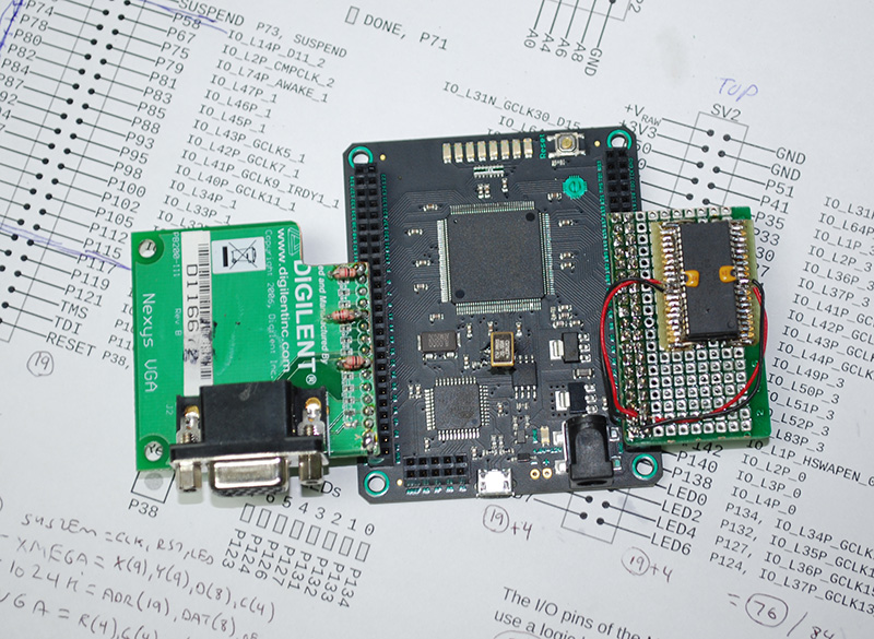
Here is the current prototype setup, hardware complete.
This should all fit nicely on a small PCB when ready...

Image
A blank 6502 computer waiting to be defined.

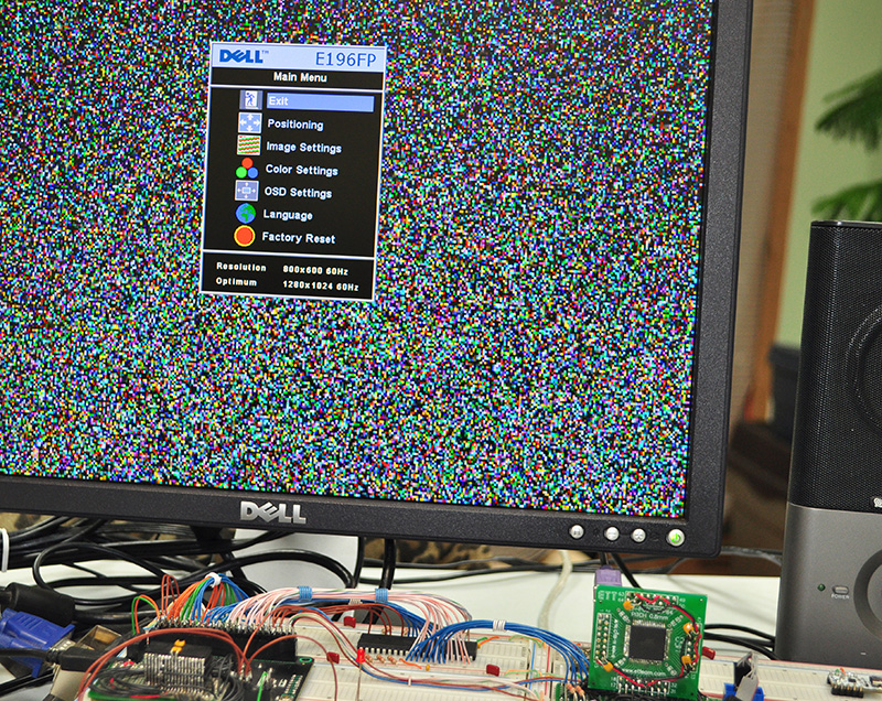
I dropped in my VGA Generator code, and redid the SRAM IO definitions.
Withing a few minutes, my monitor showed the 120,000 random pixels in the Video Buffer Memory...

Image
Hello World... GPU Style.

Now I only have to get the 6502 talking, develop an OS and IDE from scratch, and then make GPU commands.
... no problemo.

At least I can move this rig around and work on it when I have time.
Later,

Radical Brad


Top
 Profile  
Reply with quote  
PostPosted: Sun Jun 18, 2017 7:50 pm 
Offline
User avatar

Joined: Fri Aug 30, 2002 1:09 am
Posts: 8543
Location: Southern California
Oneironaut wrote:
After that, the AVR will only ever used again to send bytes from the mass storage device, probably an SD card.
I plan to make some basic command like "Set Storage Address", and "Read Byte at Address" type of thing.
The 6502 OS will have the task of turning storage data into a file structure of some kind.
The SD card will be read and written RAW as to further isolate A65 from the modern world.
We don't need no stinkin' FAT filesystem... the whole point of A65 is to be on a diet from all this modern bloat!

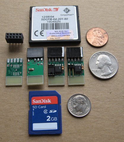
Ten months ago, I started a topic on super simple file systems for flash, at http://bradsprojects.com/forum/viewtopi ... =17&t=1233 . It's on the Brad's Projects forum rather than here since it was not 65-related, but in your case it is, so go ahead and discuss it here on 6502.org, and/or discuss over there. [Edit, spring 2022: Something about the Brad's Projects forum is broken, and Brad says he doesn't know how to fix it; so it's apparently not possible to post there now.] BDD and Ed were helpful, although I have not carried out the plan yet. I hope you do bring more discussion about it. I will be using my SPI-10 flash modules shown on the front page of my site and in the middle of this picture:
Image

Here's my first try at a 4Mx8 SRAM module, pretty much like yours:
Attachment:
4Mx8_c.jpg
4Mx8_c.jpg [ 35.92 KiB | Viewed 4648 times ]

Now of course I offer the PCB-based module on the front page of my site, with 4 ICs on each side, and the bypass capacitors in the board, under the ICs. Even though they're not stacked, the module actually takes less space this way.

_________________
http://WilsonMinesCo.com/ lots of 6502 resources
The "second front page" is http://wilsonminesco.com/links.html .
What's an additional VIA among friends, anyhow?


Top
 Profile  
Reply with quote  
PostPosted: Mon Jun 19, 2017 3:26 am 
Offline
User avatar

Joined: Mon May 25, 2015 2:25 pm
Posts: 690
Location: Gillies, Ontario, Canada
Sound good Garth. I will detail what I have in mind here as it comes together.
Hopefully some of the more sane bits of what I have planned may be of some use.
At this point, I am looking at a fixed TOC type of deal for maximum speed and ease of use.
I will probably start on BMFS (Bare Metal File System) as soon as my BMOS Assembler is working.

Speaking of that, I made HUGE progress tonight, as it started raining mid afternoon.
Some nights you think... wow, I did a lot. Some nights you go to bed frustrated.
Tonight was a good night!

This is what I managed to get done tonight...

1) The 6502 can now boot it's OS code on power up.
2) I have a workng (but very basic) IDE that can display and colorize source code.
3) The OS can do a simple assemble into another bank above the OS code space.
4) The OS can then swap to that bank and execute the assembled code.
5) The chipset can swap back to the OS when I press ESC-F1 on the keyboard.

Everything is controlled now by the 6502. There is no other processor or uC running.

I cannot edit the code in BMOS yet, just scroll around in it and then press F12 to assemble and run.
This is a great amount of progress though, as it completely proves out all of my ideas and untested code.
Most of my code was done in fragments (Verilog / 6502) in notepad on my lunch breaks!

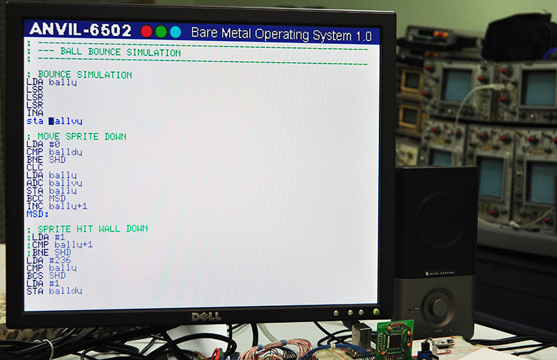
BMOS is far from done yet, but here is what gets displayed on my screen right after power up...

Image
Source code auto displayed and formatted directly from SRAM.

The square block is my flashing cursor, and it does the typical XOR type thing to the text.
All code is stored in the SRAM as a color and character byte. BMOS formats the line.

My font is not perfected yet as you can see by the cut-off small case Y on the screen.

I can scroll through 32,000 lines of code!!
That should be enough code for any 6502 program.

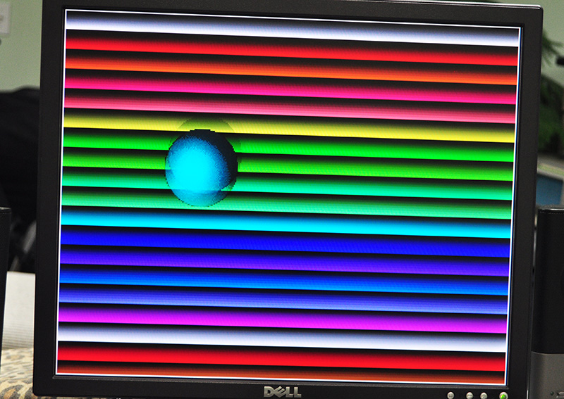
When I press F12, BMOS reads the code and assembles it to the "EXE" bank...

Image
The assembled program running in another bank in the SRAM!

The assembler is very basic at this point as well, and only about 1/4 of the 6502 instructions assemble.
It is enough to make the basic Ball Bounce Demo though.

I can't wait to get the BMOS IDE to the point where I can code directly into Anvil-6502.
At that point, I will be off the modern grid, and using the computer I dreamed of making when I was 12 years old.
Very cool!

I will post some videos next time I get the chance.

Of course, there is a LOT more do do such as the file system, SD access, full assembler, sound routines, and PCB.
If it keeps raining like this, perhaps I will actually get more done before winter arrives again!

Until next time.
Radical Brad


Top
 Profile  
Reply with quote  
PostPosted: Mon Jun 19, 2017 4:33 pm 
Offline
User avatar

Joined: Mon May 25, 2015 2:25 pm
Posts: 690
Location: Gillies, Ontario, Canada
During today's 30 minutes of free time, I have come up with a list of commands.
These are definitions inside the FPGA corrosponding to the address called by the 6502.
All Commands are memory mapped between locations 512 and 767.

Most are self explanatory....

Code:
// VIDEO COMS...
parameter COM_PAGEFLIP = 512;
parameter COM_SYNCDELAY = 513;
parameter COM_CLEARSCREEN = 514;
parameter COM_SETVGAIDX = 516;
parameter COM_SETVGALO = 517;
parameter COM_SETVGAHI = 518;
parameter COM_SETALTIDX = 519;
parameter COM_SETALTVAL = 520;

// GRAPHICS COMS...
parameter COM_SETDRAWX1LO = 521;
parameter COM_SETDRAWX1HI = 522;
parameter COM_SETDRAWY1LO = 523;
parameter COM_SETDRAWY1HI = 524;
parameter COM_SETDRAWX2LO = 525;
parameter COM_SETDRAWX2HI = 526;
parameter COM_SETDRAWY2LO = 527;
parameter COM_SETDRAWY2HI = 528;
parameter COM_SETALPHA = 529;
parameter COM_DRAWPIXEL = 530;
parameter COM_READPIXEL = 531;
parameter COM_DRAWBITMAP = 532;
parameter COM_DRAWSPRITE = 533;
parameter COM_DRAWLINE = 534;
parameter COM_DRAWFRAME = 535;
parameter COM_DRAWRECT = 536;

// TEXT COMS...
parameter COM_SETCURSX = 537;
parameter COM_SETCURSY = 538;
parameter COM_SETCHARCOLOR = 539;
parameter COM_DRAWCHAR = 540;
parameter COM_SETCODESTART = 541;
parameter COM_SETCODELENGTH = 542;
parameter COM_DRAWCODE = 543;

// KEYBOARD COMS...
parameter COM_SETKEYCHECK = 544;
parameter COM_READKEYCHECK = 750;
parameter COM_READLASTKEY = 751;

// MATH COMS...
parameter COM_SETMATHALO = 545;
parameter COM_SETMATHAHI = 546;
parameter COM_SETMATHBLO = 547;
parameter COM_SETMATHBHI = 548;
parameter COM_RUNMATHADD = 549;
parameter COM_RUNMATHSUB = 550;
parameter COM_RUNMATHMUL = 551;
parameter COM_RUNMATHDIV = 552;
parameter COM_RUNMATHSIN = 553;
parameter COM_READMATHA = 752;
parameter COM_READMATHB = 753;
parameter COM_READMATHC = 754;
parameter COM_READMATHD = 755;

// SOUND COMS...
parameter COM_SETVOXIDX = 554;
parameter COM_SETVOLUME = 555;
parameter COM_SETFREQLO = 556;
parameter COM_SETFREQHI = 557;
parameter COM_SETVOXADRA = 558;
parameter COM_SETVOXADRB = 559;
parameter COM_SETVOXADRC = 560;
parameter COM_SETVOXLENA = 561;
parameter COM_SETVOXLENB = 562;
parameter COM_SETVOXLENC = 563;
parameter COM_PLAYSOUND = 564;

// DATA COMS...
parameter COM_SETDATAREADA = 565;
parameter COM_SETDATAREADB = 566;
parameter COM_SETDATAREADC = 567;
parameter COM_SETDATAWRITEA = 568;
parameter COM_SETDATAWRITEB = 569;
parameter COM_SETDATAWRITEC = 570;
parameter COM_DATAWRITE = 571;
parameter COM_DATAREAD = 572;

// STORAGE COMS...
parameter COM_SETSTORAGEA = 573;
parameter COM_SETSTORAGEB = 574;
parameter COM_SETSTORAGEC = 575;
parameter COM_SETSTORAGED = 576;
parameter COM_STORAGEWRITE = 577;
parameter COM_STORAGEREAD = 578;

// SYSTEM COMS...
parameter COM_BANKSWITCHBMOS = 579;
parameter COM_BANKSWITCHEXE = 580;
parameter COM_RANGE1 = 580;
parameter COM_RANGE2 = 755;


Commands that are in the 750 range are "Instant Read" commands that return data to the 6502 in real time.
Since some of my functions in the FPGA will be pipelined, other reads end up in the 32 Bit Math Registers.

For instance, for the 6502 to multiply one 16 bit number by another, it has to do the following...

1) Write the 2 math input values to the following locations...
COM_SETMATHALO = 545;
COM_SETMATHAHI = 546;
COM_SETMATHBLO = 547;
COM_SETMATHBHI = 548;

2) Run the 16 by 16 multiply command...
COM_RUNMATHMUL = 551;

3) Read the 4 bytes that make up the 32 bit result...
COM_READMATHA = 752;
COM_READMATHB = 753;
COM_READMATHC = 754;
COM_READMATHD = 755;

So, this would take 5 writes and 4 reads to accomplish.
Not bad if you compare how many cycles it would take the 6502 alone to do.

Some reads are instant, such as...
COM_READKEYCHECK = 751;

This would return the last key that was pressed on the PS2 Keyboard.
In 6502 code, it would just be... LDA 751
The accumulator would now hold the ASCII value of the last key pressed.

Some of these commands are working already, and many are just fragments and ideas.
One by one, I intend to complete all of the chipset functionality until all commands are tested.

Ok, back to the modern world now...
My PC needs anther 37 gigs of updates, and I have to add 500 lines of HTML to make IE render a basic webpage properly.

Cheers!
Radical Brad


Top
 Profile  
Reply with quote  
Display posts from previous:  Sort by  
Post new topic Reply to topic  [ 83 posts ]  Go to page 1, 2, 3, 4, 5, 6  Next

All times are UTC


Who is online

Users browsing this forum: No registered users and 22 guests


You cannot post new topics in this forum
You cannot reply to topics in this forum
You cannot edit your posts in this forum
You cannot delete your posts in this forum
You cannot post attachments in this forum

Search for:
Jump to: