6502.org Forum  Projects  Code  Documents  Tools  Forum
It is currently Wed Oct 02, 2024 4:29 pm

All times are UTC


Post new topic Reply to topic  [ 12 posts ] 
Author Message
PostPosted: Sat May 13, 2017 11:35 pm 
Offline
User avatar

Joined: Wed Aug 17, 2005 12:07 am
Posts: 1228
Location: Soddy-Daisy, TN USA
So, I have a little 65C02 soldered up on a protoboard.

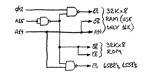
I am using the address decoding from the primer (16K RAM, 32K ROM).

Here: http://wilsonminesco.com/6502primer/addr_decoding.html

Image

Next, I loaded my ROM with 32K of $EA.

I then have a frequency generator outputting a 1KHz square wave on PHI2.

The wave appears to be perfect going into the CPU.

The data bus shows the correct $EA values on each pin.

However, every pin on the address bus is 5V. All of them. The scope shows no oscillation on the address pins. I would have thought A0 would have shown a square wave of 250 Hz.

Now, the weird part is PHI1O (pin 3) of the CPU is a flat 5V (no oscillation) and PHI2O (pin 39) is a flat 0V (no oscillation).

It's like the CPU isn't running at all.

I have 3.3K pull-ups on: RDY, IRQ, NMI, RESET, SOB and BE.

I have a pretty good reset switch tied between RESET and GND.

The scope shows 5V on the RESET line and when I press the button it has a nice drop to GND. So reset should be good.

Any idea what I'm missing? I've checked the pins with my multimeter and they all appear to be correct.

What would cause the CPU to not step through?

Thanks.

_________________
Cat; the other white meat.


Top
 Profile  
Reply with quote  
PostPosted: Sat May 13, 2017 11:51 pm 
Offline
User avatar

Joined: Wed Mar 01, 2017 8:54 pm
Posts: 660
Location: North-Germany
Sounds not good.
Do you have a second unit to test?


Top
 Profile  
Reply with quote  
PostPosted: Sun May 14, 2017 12:57 am 
Offline
User avatar

Joined: Thu May 28, 2009 9:46 pm
Posts: 8410
Location: Midwestern USA
cbmeeks wrote:
So, I have a little 65C02 soldered up on a protoboard...I then have a frequency generator outputting a 1KHz square wave on PHI2.

A couple of things come to mind. One is the signal generator's output must swing from zero to nearly Vcc, which is Vcc at the 65C02. Specifically, your Ø2 input must reach a minimum of Vcc × 0.7 volts to be recognized as a valid high, and sink to at least Vcc × 0.2 to qualify as a valid low (the data sheet says Vcc × 0.3, but I suspect that is in error). These should be considered "ragged edge" limits. Are you sure you are meeting these requirements?

What's the rise and fall time on that square wave? Ideally it should be 5ns or less. I recall a caveat somewhere about the WDC versions of the 65C02 malfunctioning when subjected to slow transitions on the clock input. It has nothing to do with input frequency. If your generator's output cannot meet the 5ns transition rate try introducing a 74AC74 flip-flop between the generator and Ø2 in, with the generator set to 2KHz.

While looking at the Ø1 and Ø2 outputs is useful to see if the MPU's clock circuitry is alive, you should keep in mind that the timing relationships between the Ø2 input and the Ø1 and Ø2 outputs of the 65C02 are not specified by WDC, and are not tested during production. All that is assured is that the Ø1 and Ø2 outputs will lag the Ø2 input by some amount. There is also no assurance that the Ø2 output is exactly 180 degrees out of phase with the Ø1 output. These outputs should not be used in new designs and are present only to support in-circuit replacement of an NMOS 6502.

Also, you need to do something to debounce the release of the reset push button. Note that Ø2 must be stable before reset is toggled.

_________________
x86?  We ain't got no x86.  We don't NEED no stinking x86!


Top
 Profile  
Reply with quote  
PostPosted: Sun May 14, 2017 3:07 am 
Offline
User avatar

Joined: Wed Aug 17, 2005 12:07 am
Posts: 1228
Location: Soddy-Daisy, TN USA
Thanks for the tips!

BigDumbDinosaur wrote:
One is the signal generator's output must swing from zero to nearly Vcc, which is Vcc at the 65C02. Specifically, your Ø2 input must reach a minimum of Vcc × 0.7 volts to be recognized as a valid high, and sink to at least Vcc × 0.2 to qualify as a valid low (the data sheet says Vcc × 0.3, but I suspect that is in error). These should be considered "ragged edge" limits. Are you sure you are meeting these requirements?


I think that was it. The frequency generator had 5V P2P. However, my scope was showing a low of 1.xV and a high of 6V or so. Not sure why that was happening.

So I put in a plain-jane 1MHz canned oscillator and discovered that A0 was running an average of 250 KHz. Which is what I expected! But I'm a little stumped. I've used my frequency generator to drive other chips. Including AY-3-8910's before with 0 issues. I guess it just isn't putting out enough current that the 'C02 needs?


BigDumbDinosaur wrote:
While looking at the Ø1 and Ø2 outputs is useful to see if the MPU's clock circuitry is alive, you should keep in mind that the timing relationships between the Ø2 input and the Ø1 and Ø2 outputs of the 65C02 are not specified by WDC, and are not tested during production.


Right. I wouldn't use them in a modern design. I was just hoping they would tell me if the 'C02 was clocking or not. I would imagine (maybe incorrectly) that in a proper circuit, they should be doing SOMETHING other than flat-lining. :-)

Anyway, I feel better now that my test circuit seems to be free-running. Now on to soldering in some I/O.

On a different topic, I only have a few '00 NAND's on hand. I have some 74AC00's and some 74LS00's. I know the LS series is frowned upon on modern designs. I've also read they *should* be OK for low frequency...low drive stuff. The only thing I am using the NAND for is the aforementioned circuit.

So, I originally had the 74AC00 in the circuit but I noticed the "GND reference" signal of the square wave had TONS of bounce...for a lack of better terms. The peak frequency looked OK but the low signal looked like a sawtooth wave. When I swapped it out for the 74LS00, the entire wave (up to 1MHz) looked almost perfect.

Now, granted, that was when I was using the frequency generator. But what I'm puzzled about is why the AC version made the wave so much "dirtier" than the LS version?

I may swap it out again and see if the canned oscillator does the same thing.

Thanks!

_________________
Cat; the other white meat.


Top
 Profile  
Reply with quote  
PostPosted: Sun May 14, 2017 3:38 am 
Offline
User avatar

Joined: Fri Aug 30, 2002 1:09 am
Posts: 8521
Location: Southern California
cbmeeks wrote:
I think that was it. The frequency generator had 5V P2P. However, my scope was showing a low of 1.xV and a high of 6V or so. Not sure why that was happening.

So I put in a plain-jane 1MHz canned oscillator and discovered that A0 was running an average of 250 KHz. Which is what I expected! But I'm a little stumped. I've used my frequency generator to drive other chips. Including AY-3-8910's before with 0 issues. I guess it just isn't putting out enough current that the 'C02 needs?

It sounds like you had an offset dialed in, if it was going from 1.x-6V instead of 0-5V. The 65c02's input is CMOS, so the only current it needs is the tiny amount to charge the capacitance in the input gates and the leadframe.

Quote:
On a different topic, I only have a few '00 NAND's on hand. I have some 74AC00's and some 74LS00's. I know the LS series is frowned upon on modern designs. I've also read they *should* be OK for low frequency...low drive stuff. The only thing I am using the NAND for is the aforementioned circuit.

LS's inputs present a much heavier load to any signal line than CMOS (HC, HCT, AC, ACT, etc.), and its output cannot pull up very high, and in fact may not be dependable to get up high enough for a solid logic '1' for CMOS inputs. I've used LS in a pinch, without problems, but also knowing that I didn't have much margin to keep it working.

Quote:
But what I'm puzzled about is why the AC version made the wave so much "dirtier" than the LS version?

It's because the slew rate is so much faster on the AC than it is on the LS, and that faster rate of change in output current, times the inductance in the ground circuit, makes for a higher voltage at the ground pin.

_________________
http://WilsonMinesCo.com/ lots of 6502 resources
The "second front page" is http://wilsonminesco.com/links.html .
What's an additional VIA among friends, anyhow?


Top
 Profile  
Reply with quote  
PostPosted: Sun May 14, 2017 7:14 am 
Offline
User avatar

Joined: Thu May 28, 2009 9:46 pm
Posts: 8410
Location: Midwestern USA
cbmeeks wrote:
I think that was it. The frequency generator had 5V P2P. However, my scope was showing a low of 1.xV and a high of 6V or so. Not sure why that was happening.

So I put in a plain-jane 1MHz canned oscillator and discovered that A0 was running an average of 250 KHz. Which is what I expected! But I'm a little stumped. I've used my frequency generator to drive other chips. Including AY-3-8910's before with 0 issues. I guess it just isn't putting out enough current that the 'C02 needs?

As Garth noted, the CMOS inputs of the 65C02 represent negligible loading, other than the capacitance. Your signal generator probably was not meeting the rise and fall times required by the 'C02.

Quote:
BigDumbDinosaur wrote:
While looking at the Ø1 and Ø2 outputs is useful to see if the MPU's clock circuitry is alive, you should keep in mind that the timing relationships between the Ø2 input and the Ø1 and Ø2 outputs of the 65C02 are not specified by WDC, and are not tested during production.

Right. I wouldn't use them in a modern design. I was just hoping they would tell me if the 'C02 was clocking or not. I would imagine (maybe incorrectly) that in a proper circuit, they should be doing SOMETHING other than flat-lining. :-)

You should be able to see output on those pins, so they are usable as diagnostic points.

Quote:
So, I originally had the 74AC00 in the circuit but I noticed the "GND reference" signal of the square wave had TONS of bounce...for a lack of better terms. The peak frequency looked OK but the low signal looked like a sawtooth wave. When I swapped it out for the 74LS00, the entire wave (up to 1MHz) looked almost perfect.

Now, granted, that was when I was using the frequency generator. But what I'm puzzled about is why the AC version made the wave so much "dirtier" than the LS version?

As Garth pointed out, you are seeing the effects of rapid output transition. In some cases, 74AC logic can approach sub-nanosecond output transition rates, as well as produce strong output drive (usually sourcing and sinking 24mA in a 5 volt system). These characteristics, as well as very short propagation time, make 74AC logic perform well in fast systems. My POC V1.1, for example, using all 74AC logic, will boot at 15 MHz on a 45ns ROM, and I'm sure, would operate at 20 MHz if I had wait-state hardware.

However, the extremely rapid output state transition characteristic of 74AC devices generates a huge amount of high order harmonic content, causing momentary but very intense transients at the Vcc and ground connections of the device. You counteract the effects of those transients with a suitable decoupling capacitor (a 0.1µF X7R MLCC, with a 50 volt rating is a good choice) and a robust ground connection.

The capacitor must be as physically close to the device as possible, with the Vcc connection as physically short as possible. I design my PCB layouts so the path from the Vcc inner layer to the device proper is through the capacitor's pad so the capacitor is electrically "in between" the device and the Vcc rail (a design feature I saw years ago in an MC68000 minicomputer). That gives the capacitor every possibility to capture and dissipate any switching transients before they get onto the Vcc inner layer. You can do something similar on a hand-wired unit if you are careful.

On the ground side, you need to keep inductance out of the picture as much as possible with short and direct connections. The ideal way to achieve this on a PCB is with an inner ground plane, which is what I use in my POC designs. That isn't possible with proto-board, so you need to plan carefully.

Wire size doesn't have much to do with it. It's mostly length between the power source and the power consumer that matters. Much more than few inches and you are likely to get into induced ground bounce, in which the ground connection at the device is momentarily above ground potential as the device's output state changes. If the effective difference between the ground pin and an input pin changes enough due to ground bounce, the device will become confused by what it is seeing at the input and in some cases may go into oscillation. Needless to say, that would be bad, very bad. :twisted:

There's quite a bit of discussion around here about construction techniques with high speed logic. Garth also goes into it on his website. Succinctly stated, Vcc and ground connections need to be as short and direct as possible and well bypassed, with an MLCC at each device and low-ESR electrolytics in strategic locations to help stabilize Vcc.

Quote:
I may swap it out again and see if the canned oscillator does the same thing.

You may see an improvement. Let us know...
_________________
x86?  We ain't got no x86.  We don't NEED no stinking x86!


Top
 Profile  
Reply with quote  
PostPosted: Mon May 15, 2017 1:17 pm 
Offline
User avatar

Joined: Wed Aug 17, 2005 12:07 am
Posts: 1228
Location: Soddy-Daisy, TN USA
BigDumbDinosaur wrote:
The capacitor must be as physically close to the device as possible, with the Vcc connection as physically short as possible. I design my PCB layouts so the path from the Vcc inner layer to the device proper is through the capacitor's pad so the capacitor is electrically "in between" the device and the Vcc rail (a design feature I saw years ago in an MC68000 minicomputer). That gives the capacitor every possibility to capture and dissipate any switching transients before they get onto the Vcc inner layer. You can do something similar on a hand-wired unit if you are careful.


You know, that's the way I've always done it after reading years ago that the cap should be as close as possible.

So, I get a little surprised when I see wire-wrapped computers (from people I respect) to even commercial computers like the C64 that sometimes put the cap at the TOP of the IC (centered) instead of right next to the VCC pin. I always try to put the cap right on the VCC pin when I can.

_________________
Cat; the other white meat.


Top
 Profile  
Reply with quote  
PostPosted: Mon May 15, 2017 1:38 pm 
Offline
User avatar

Joined: Thu Dec 11, 2008 1:28 pm
Posts: 10943
Location: England
"As close as possible" never has made sense to me. All engineering is tradeoffs. What is meant here is that close is good, distant is bad. An absolute beginner who knows only that wires conduct electricity would feel OK about putting just one capacitor in the corner of the board where the power arrives - I know I would have done. And it's useful to correct that. But it's possible to overdo the advice to the point that it's off putting. Or indeed to the point that it's not even good advice - it's possible to solder a capacitor directly to the pins, if the pins happen to be adjacent, but it's very rarely done, and all the designs which don't do that, they are fine too.


Top
 Profile  
Reply with quote  
PostPosted: Mon May 15, 2017 5:04 pm 
Offline
User avatar

Joined: Tue Nov 16, 2010 8:00 am
Posts: 2353
Location: Gouda, The Netherlands
I think best advice for beginners: use 1 or 2 MHz, and avoid AC series. That makes everything else a lot less critical.


Top
 Profile  
Reply with quote  
PostPosted: Mon May 15, 2017 8:25 pm 
Offline
User avatar

Joined: Fri Aug 30, 2002 1:09 am
Posts: 8521
Location: Southern California
cbmeeks wrote:
So, I get a little surprised when I see wire-wrapped computers (from people I respect) to even commercial computers like the C64 that sometimes put the cap at the TOP of the IC (centered) instead of right next to the VCC pin. I always try to put the cap right on the VCC pin when I can.

I wish they hadn't set a standard decades ago of putting power and ground at opposite corners. They should have been in the middle, where the internal connections between the pin and the die are the shortest. But since we are stuck with the opposite-corners standard for 74xxxx, soldering a capacitor to the top on the IC, to its pins, is a good way to go, and keep the leads as straight and direct and short as possible. Beyond that, it does not matter how much of the lead length is on one side of the capacitor and how much on the other, because it's all in series. You could put the capacitor's body nearly touching the Vcc pin, and then you have all the lead length (which has inductance) between the other side of the capacitor and the IC's ground pin, and it wouldn't be any better than centering the capacitor, or putting it close to the ground pin. (BTW, soldering a capacitor to the IC's leads themselves is something I have seldom done.)

Unfortunately then you still have inductance in the socket and between ICs, but we do the best we can with what we know, and get reasonable degrees of success.

_________________
http://WilsonMinesCo.com/ lots of 6502 resources
The "second front page" is http://wilsonminesco.com/links.html .
What's an additional VIA among friends, anyhow?


Top
 Profile  
Reply with quote  
PostPosted: Mon May 15, 2017 10:18 pm 
Offline
User avatar

Joined: Thu May 28, 2009 9:46 pm
Posts: 8410
Location: Midwestern USA
GARTHWILSON wrote:
I wish they hadn't set a standard decades ago of putting power and ground at opposite corners. They should have been in the middle, where the internal connections between the pin and the die are the shortest.

Centralized Vcc and ground connections in DIP became more common when speeds were jacked up in the 1990s, but of course, 74xx packages couldn't be changed.

Note how Cypress, for example, centralized Vcc and ground in their 512KB SRAM, which has good and bad elements to it. The good part is if using a multilayer board with internal ground and power planes, you've got a very short and direct path from the die to the power/ground layers, which means the SRAM sees a more stable Vcc source, and ground bounce is greatly curtailed.

The bad is that on a two-layer board you've got those connections smack in the middle between address and data pins, which complicates routing.

_________________
x86?  We ain't got no x86.  We don't NEED no stinking x86!


Top
 Profile  
Reply with quote  
PostPosted: Mon May 15, 2017 11:03 pm 
Offline
User avatar

Joined: Fri Aug 30, 2002 1:09 am
Posts: 8521
Location: Southern California
The Cypress 512KB SRAM is used on my memory modules. They went further, putting a ground and a Vcc together on each side. Nice!

Here's a capacitor soldered to adjacent power & ground pins, something I did on a PIC microcontroller a few years ago:
Attachment:
PICcap.jpg
PICcap.jpg [ 93.62 KiB | Viewed 3810 times ]

Here's one we had to do on a production run of boards in about 1994. After this run was assembled, we found out that Maxim changed the wafer process and increased the slew rate on the switching in this switching power supply controller, causing ringing and other problems that made a lot of electrical noise that got into the aircraft radios. Rather than scrap the whole lot and not having anything to sell until the board could be re-designed, we reworked them by hand, putting this capacitor on the top of the 8-pin IC, making the shortest connection we could between the capacitor and the die of the IC. (The die is the actual chip inside the IC.) It worked well.
Attachment:
MAX732capScab.jpg
MAX732capScab.jpg [ 43.43 KiB | Viewed 3810 times ]

Although I used the same IC on subsequent designs, I did the board layout different. The last one was six or eight years ago; and although much of the board was surface-mount, the space was very limited, and I couldn't get fit SMT version of the IC in, but I could get the thru-hole one in, because I could put chip capacitors underneath it, between the board and the body of the IC, with the connections as short as possible. Operation was very quiet and stable. (The SMT version didn't leave enough space underneath to put the chip capacitors.)

BigDumbDinosaur wrote:
The bad is that on a two-layer board you've got those connections smack in the middle between address and data pins, which complicates routing.

True, and when 7400 TTL was first out, I imagine 2-layer boards were not very common. In my early days of electronics as a poor paper boy who had to take apart old and surplus electronics to get parts, I remember even logic boards that were single-sided. As a side note, apparently thru-plating wasn't very reliable yet, and sometimes hollow rivets were used for the purpose.

_________________
http://WilsonMinesCo.com/ lots of 6502 resources
The "second front page" is http://wilsonminesco.com/links.html .
What's an additional VIA among friends, anyhow?


Top
 Profile  
Reply with quote  
Display posts from previous:  Sort by  
Post new topic Reply to topic  [ 12 posts ] 

All times are UTC


Who is online

Users browsing this forum: No registered users and 7 guests


You cannot post new topics in this forum
You cannot reply to topics in this forum
You cannot edit your posts in this forum
You cannot delete your posts in this forum
You cannot post attachments in this forum

Search for:
Jump to: