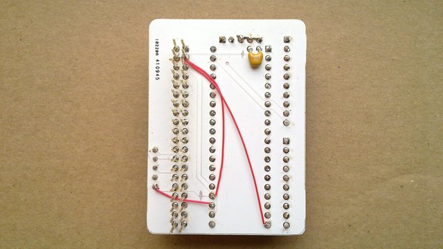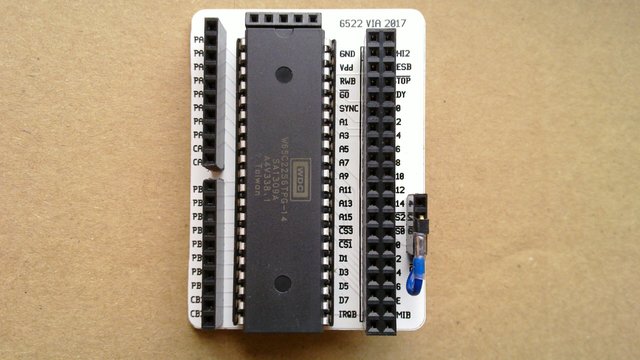
I'm used to seeing supply pins labelled VCC and GND in data sheets, but when I saw VSS and VDD in the W65C22 data sheet I thought I'd use the correct labels from the data sheet in my schematic symbol. I've been making PCBs for a while now, so often I go straight to a PCB rather than prototyping and drew a schematic then laid out a PCB for the VIA based on the net list and then ordered the board. The PCB arrived, and I assembled it. It was then that I realised I'd wired the /CSx line from the bus to CS1 rather than to CS2B (which I'd wired to GND). The VIA would have been selected every time I didn't address it and not when I did. After the rework, I inserted the module in to my system, which failed to boot. After about ten seconds I checked the VIA with a finger and found it warm, so I powered down and looked for faults in my schematic. That's when I noticed that I'd designed the circuit with the VSS pin wired to +3V3 and VDD to GND. Epic fail. I reworked the board but knew that I'd damaged the VIA. I didn't think I could lose anything by trying it anyway. The system booted, which was a good sign. Then I dumped the registers (the VIA is mapped between $E120..$E12F at the moment):
Code: Select all
Neil's 6502 SBC R2
64K RAM SYSTEM
READY
SP:ff
> de120
e120  00 00 00 00 9b b8 bb fb 9e ea ff 00 00 00 80 00-
e130  3e fd 8c eb a6 63 cb ae fb c9 31 fc e2 f0 36 2f-
I was lucky this time but in future I think I'll prototype and/or check my schematic more carefully (at least until the next time I get overconfident).
Not as pretty as I'd hoped:

But can't tell from the top:
