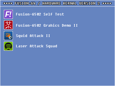
From here on, it will be referred to as FFS (Fusion File System).
Cartridges (SPI Flash Memories) are going to hold multiple programs and multiple data files, and the capacity will range from a few hundred megs to several gigs.
The flash will be written to via PC USB link directly to the Fusion system. A program I made to develop games and demos will do all the work.
There will be a single file called The TOC starting at location zero, and it will be a total of 64K in size.
In the TOC, there will be 41 byte entries defining files on the flash as so...
File Name : 32 Bytes (Fixed length alpha-numeric)
File Type : 1 Byte (0:Program / 1:Data)
File Start : 4 bytes (32 bit address value)
File Length : 4 Bytes (32 bit length value)
Since the TOC is 65536 bytes long, and a file entry is 41 bytes long, the TOC will be able to hold 1598 entries, which is more than enough.
I will probably just cap this to 1024 entries, since I like things to fit into byte sets.
All program Files will be exactly 64,768 Bytes in size, which is the full 64K memory space minus zero page, stack, and IO space.
Data files can be any length at all, up to 4,294,967,296 bytes in size due to the 32 bit addressing used.
When Fusion-64 boots, the FPGA will stuff the menu program into the 6502 program space, and then the 6502 will look for the SPI memory.
If a cartridge is present, it will read the TOC, and then stream all of the file names (programs only) to a place in the main working SRAM.
From there, the 6502 will draw up a boot menu where it will allow joystick navigation through the program files (not data files).
The user can then select a program and press fire to load it.
Once up and running, the program can refer to the loaded file table to gain location information on Data Files it may need to access.
There will be no writing from Fusion-64 to the Flash Memory, just reading.
The PC program will handle all writing of data, which will include compiled 6502 programs, sounds, and graphics.
I have had limited time, but managed to get text modes working, and added a Line Drawing function to the FPGA.
I will use lines and text to create a simple boot screen, which will also include a centering border and color test pattern.
I wanted to post more than just me yapping about this project, so here is the latest GPU function.
This is Verilog code that will draw a single pixel line from X1,Y1 to X2,Y2.
Although I hacked it about, one might still recognize Bresenham's line algorithm in here....
Code: Select all
///////////////////////////////////////////////////////////////////////////////////////////////////////////////////////////////////////////////////////////////////
////////// COMMAND 542 : DRAW LINE USING DRAWX1, DRAWY1, DRAWX2, DRAWY2
////////// DATA : LINE COLOR VALUE
///////////////////////////////////////////////////////////////////////////////////////////////////////////////////////////////////////////////////////////////////

// CALCULATE LINE DELTAS
if (COMMAND == 542 & COMSTEP == 1) begin
if (DRAWX1 > DRAWX2) DELTAX <= DRAWX1 - DRAWX2;
if (DRAWX1 < DRAWX2) DELTAX <= DRAWX2 - DRAWX1;
if (DRAWY1 > DRAWY2) DELTAY <= DRAWY1 - DRAWY2;
if (DRAWY1 < DRAWY2) DELTAY <= DRAWY2 - DRAWY1;
TEMPX <= DRAWX1;
TEMPY <= DRAWY1;
TEMPL <= 0;
COMSTEP <= 2;
end

// CALCULATE LINE STEPS
if (COMMAND == 542 & COMSTEP == 2) begin
if (DELTAX >= DELTAY) begin
LINELEN <= DELTAX;
DELTAQ <= (DELTAY >> 1) - DELTAX + 1024;
DINC1 <= DELTAY << 1;
DINC2 <= (DELTAX - DELTAY) << 1;
XINC1 <= 1;
XINC2 <= 1;
YINC1 <= 0;
YINC2 <= 1;
end else begin
LINELEN <= DELTAY;
DELTAQ <= (DELTAX >> 1) - DELTAY + 1024;
DINC1 <= DELTAX << 1;
DINC2 <= (DELTAY - DELTAX) << 1;
XINC1 <= 0;
XINC2 <= 1;
YINC1 <= 1;
YINC2 <= 1;
end
COMSTEP <= 3;
end

// SEND PIXEL LOCATION AND COLOR VALUE
if (COMMAND == 542 & COMSTEP == 3 & MEMREADY == 1) begin
if (TEMPX < 400 & TEMPY < 300) begin
SRAMSEND <= COMDATA;
SRAMADR <= TEMPX + (TEMPY * 400) + DRAWPAGE;
SRAMWE <= 0;
end
COMSTEP <= 4;
end

// NEXT LINE POINTS
if (COMMAND == 542 & COMSTEP == 4) begin
if (DELTAQ < 1024) begin
DELTAQ <= DELTAQ + DINC1;
if (DRAWX1 < DRAWX2) TEMPX <= TEMPX + XINC1;
if (DRAWX1 > DRAWX2) TEMPX <= TEMPX - XINC1;
if (DRAWY1 < DRAWY2) TEMPY <= TEMPY + YINC1;
if (DRAWY1 > DRAWY2) TEMPY <= TEMPY - YINC1;
end else begin
DELTAQ <= DELTAQ - DINC2;
if (DRAWX1 < DRAWX2) TEMPX <= TEMPX + XINC2;
if (DRAWX1 > DRAWX2) TEMPX <= TEMPX - XINC2;
if (DRAWY1 < DRAWY2) TEMPY <= TEMPY + YINC2;
if (DRAWY1 > DRAWY2) TEMPY <= TEMPY - YINC2;
end
TEMPL <= TEMPL + 1;
if (TEMPL < LINELEN) begin
COMSTEP <= 3;
end else begin
COMSTEP <= 255;
end
end
... yeah, it is!
Just remember... every line of code executes on every clock cycle.
I use "COMSTEP" to sort that confusion out.
Also note the use of "MEMREADY", which only allows the SRAM OE pin to go low when it is true.
The line is drawn at a rate of 20,000 pixels per second, since it takes 2 cycles for each iteration.
I am going to optimize this more, and may be able to get it running at the full 40MHz clock speed.
Once I can scrounge up an SPI Flash chip and an FT232 chip, I will do the hardware interface between the PC.
For now, I am stuck with stuffing 6502 code into the FPGA and then waiting for the 5 minute synthesis time!
Life would also be easier if Verilog had an "Include" function that worked like any other IDE!
Later,
Brad
