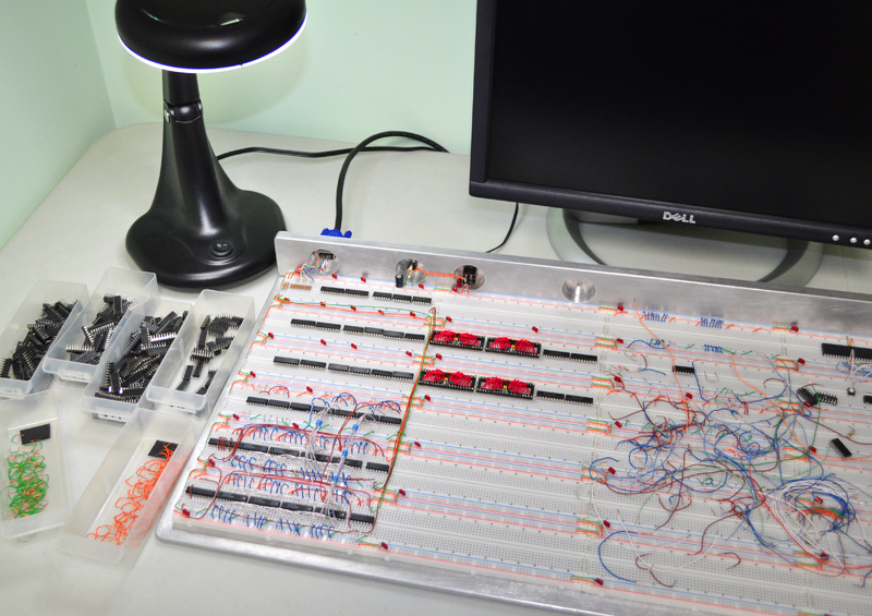
I would like to build one of those to play with it . Is there any chance to share the latest verilog and 6502 code with us ? .
Thank you .
I am just working on the Sound Engine now, and so far it's coming along nicely.
I also added Text using the C64 character set.
This may sound strange, but I have decided to make the schematics and BIT files freely available, but do not plan on releasing my HDL source.
I will however, but adding a COMPLETE tutorial on how to get started on this kind of thing and how to carve out a working FPGA project.
Code examples will be presented in segments, showing how it all works, for example; VGA generation, 6502 Interface, SRAM interfacing, etc.
My reasons...
- I want "Fusion-6502" to be all about the 6502, and NOT the FPGA. The FPGA is just a black box chip-set to do video and sound.
- My methods of coding Verilog are so far beyond the accepted standards that I simply don't want the drama. And there would be a LOT!
Some of my own personal HDL rules...
- Never use simulations, debuggers, or test-benches. Ever.
- Never use modules. All code is on one SINGLE @always edge block only.
- Never us IP, cores, or pre-made code. All code is made 100% from scratch.
- Never learn from others code examples. Datasheets vs trial and error only.
- All values in code are represented as decimal. No HEX, Octal, or Binary.
- Designs to be stable without requiring an external reset. Use of "Initial Begin" required.
- Define all states, and never waste a bit.
My design rules work extremely well personally, but would get you fired professionally!
Just sayin'... hackers like myself are not generally welcome in most FPGA / HDL forums.
If you intend to work professionally or collaborate, then it would be better to follow standards.
Last time I shared some HDL, I had all the experts in such a tizzy that the thread exploded for 2 weeks describing possible reason why my project would fail to ever work, and why everything I did was completely ridiculous. By the time the storm subdued, I was already into V3 of my board and code, which by the way is now used in a commercial touch screen product!
Anyhow, I will certainly put a lot of effort into teaching what I have learned about graphics and Verilog when I have the chance, but it will be more of a step by step tutorial on VGA basics, SRAM interfacing, and getting speed out of an FPGA design. My LucidScience site is in dire need of a complete redo, as all my projects are dated, and this will be one of the new ones.
From here on, I will be focusing on this project with the 6502 in mind, as the FPGA is nothing more than a powerslave.
Brad


