
Would that be this article from August 1982? (That's the Logo issue.)
"High-Resolution Sprite-Oriented Color Graphics" by Steve Ciarcia
Looks good!
Interfacing stock 6502 to TMS9918

Re: Interfacing stock 6502 to TMS9918
Actually at this moment I need simple examples just to test the display. I've hooked up the sram interface and simple test of writing to and reading from vram has failed at the moment. I should check the wiring on the breadboard.
But for the future of course it would be more than fine to have some kind of commented sources The ones from datasheet are like gibberish since coded in tms assembly.
But for the future of course it would be more than fine to have some kind of commented sources
Re: Interfacing stock 6502 to TMS9918
i_r_on wrote:
Actually at this moment I need simple examples just to test the display. I've hooked up the sram interface and simple test of writing to and reading from vram has failed at the moment. I should check the wiring on the breadboard.
I've not used the 9918, but I would guess it is similar to the 9938/9958. From the datasheet it looks broadly the same but simpler due to only supporting 32KB? of DRAM, less video modes etc. Start with a routine to write to an arbitrary register; two bytes on A0=1, first byte is the value second byte is the register, with bits 10000CBA, where C B A is the register "address". Another routine to read the status register might be useful.
Then you'll want two routines, one to read and one to write to the VRAM. I wouldn't even bother to hook up a TV until this is working. Actually, I'd probably get this working before doing the register reading and writing.
Good luck.
8 bit fun and games: https://www.aslak.net/
Re: Interfacing stock 6502 to TMS9918
For those that are interested, I uploaded all of my PDF files for the various TMS9918 chips. Including one that tells you how to replace the DRAM with an SRAM.
https://github.com/cbmeeks/TMS9918
https://github.com/cbmeeks/TMS9918
Cat; the other white meat.
Re: Interfacing stock 6502 to TMS9918
Thanks for doing that!
Re: Interfacing stock 6502 to TMS9918
Share the wealth is what I always say. 
Cat; the other white meat.
Re: Interfacing stock 6502 to TMS9918
@Aslak3 : Sram interface is in the link below.
http://retrobrewcomputers.org/n8vem-pbw ... 20VRAM.pdf
The issue with DRAMs is they are hard to be found and eight 4116 chips are needed. Another issue is 4116 chips need -5V and -12V power rails. First I thought I could get away with 4416 chips but those chips are not compatible with TMS VDC. TMS needs separate unidirectional bus on the DRAM chip since it's VRAM interface is not bidirectional. 4116 chips have input D and output Q separately where as 4416 chips have them together.
9918 and it's variants supports 4K or 16K ram. 9958 is much more complicated chip but I guess it's software compatible with 9918.
Actually I already wrote the arduino code to interface to the chip. It's somewhat working but has issues somehow. I need to check the connections.
One question comes to mind, Is A14..A0 in the address setup phase, are those too inverse to standard notation? A0 is MSB and A14 is LSB?
Here is the code I use to interface to the chip
@cbmeeks : Thanks for the documents!
http://retrobrewcomputers.org/n8vem-pbw ... 20VRAM.pdf
The issue with DRAMs is they are hard to be found and eight 4116 chips are needed. Another issue is 4116 chips need -5V and -12V power rails. First I thought I could get away with 4416 chips but those chips are not compatible with TMS VDC. TMS needs separate unidirectional bus on the DRAM chip since it's VRAM interface is not bidirectional. 4116 chips have input D and output Q separately where as 4416 chips have them together.
9918 and it's variants supports 4K or 16K ram. 9958 is much more complicated chip but I guess it's software compatible with 9918.
Actually I already wrote the arduino code to interface to the chip. It's somewhat working but has issues somehow. I need to check the connections.
One question comes to mind, Is A14..A0 in the address setup phase, are those too inverse to standard notation? A0 is MSB and A14 is LSB?
Here is the code I use to interface to the chip
Code: Select all
#define MODE 2
#define CSW 3
#define CSR 8
#define RESET 9


#define PORT_MANIPULATION

int bytePins[8] =   { 14, 15 , 16, 17, 4, 5, 6, 7 };

void setDBReadMode() {
  #ifdef PORT_MANIPULATION
  DDRD = DDRD & B00001111; // Set Pin 4..7 as inputs. High nibble of databus.
  DDRC = DDRC & B11110000; // Set Analog pin 0..3 as inputs
  #else
  for (int i=0;i<8;i++) {
    pinMode(bytePins[i], INPUT);
  }
  #endif
}

void setDBWriteMode() {
  #ifdef PORT_MANIPULATION
  DDRD = DDRD | B11110000; // Set Pin 4..7 as outputs. High nibble of databus.
  DDRC = DDRC | B00001111; // Set Analog pin 0..3 as outputs
  #else
  for (int i=0;i<8;i++) {
    pinMode(bytePins[i], OUTPUT);
  }
  #endif
}

void reset() {
  Serial.println("Resetting");
  digitalWrite(RESET, HIGH);
  delayMicroseconds(100);
  digitalWrite(RESET, LOW);
  delayMicroseconds(5);
  digitalWrite(RESET, HIGH);
}

inline void setPort(unsigned char value) {
    #ifdef PORT_MANIPULATION
    PORTD = (PIND & 0x0F) | (value & 0xF0);
    PORTC = (PINC & 0xF0) | (value & 0x0F);
    #else
    unsigned char mask = 1;
    for (int i=0;i<8;i++) {
      digitalWrite(bytePins[i], value & mask);
      mask = mask<<1;
    }
    #endif
}

inline unsigned char readPort() {
    unsigned char memByte = 0;
    #ifdef PORT_MANIPULATION
    memByte  = (PIND & 0xF0) | (PINC & 0x0F);
    #else
    unsigned char mask = 1;
    for (int i=0;i<8;i++) {
      if (digitalRead(bytePins[i])) {
        memByte = memByte | mask;
      }
      mask = mask<<1;
    }
    #endif

    return memByte;
}

//Writes a byte to databus for register access
void writeByte( unsigned char value) {
    setDBWriteMode();
    setPort(value);
    digitalWrite(MODE, HIGH);
    digitalWrite(CSW, LOW);
    delayMicroseconds(10);
    digitalWrite(CSW, HIGH);
    setDBReadMode();
}

//Reads a byte from databus for register access
unsigned char  readByte( ) {
    unsigned char memByte = 0;
    digitalWrite(MODE, HIGH);
    digitalWrite(CSR, LOW);
    delayMicroseconds(10);
    memByte = readPort();
    digitalWrite(CSR, HIGH);
    return memByte;
}

//Writes a byte to databus for vram access
void writeByteToVRAM( unsigned char value) {
    setDBWriteMode();
    setPort(value);
    digitalWrite(MODE, LOW);
    digitalWrite(CSW, LOW);
    delayMicroseconds(10);
    digitalWrite(CSW, HIGH);
    setDBReadMode();
}

//Reads a byte from databus for vram access
unsigned char  readByteFromVRAM( ) {
    unsigned char memByte = 0;
    digitalWrite(MODE, LOW);
    digitalWrite(CSR, LOW);
    delayMicroseconds(8);
    memByte = readPort();
    digitalWrite(CSR, HIGH);
    return memByte;
}

void setRegister(unsigned char registerIndex, unsigned char value) {
  writeByte(value);
  writeByte(0x80 | registerIndex);
}

void setWriteAddress( unsigned int address) {
  writeByte((address & 0xFFC0)>>6);
  writeByte(0x40 | (address & 0x3F));
}

void setReadAddress( unsigned int address) {
  writeByte((address & 0xFFC0)>>6);
  writeByte((address & 0x3F));
}

void setup() {
  setDBReadMode();
  Serial.begin(9600);
  pinMode(MODE, OUTPUT);
  pinMode(RESET, OUTPUT);
  pinMode(CSW, OUTPUT);
  pinMode(CSR, OUTPUT);

  digitalWrite(RESET, HIGH);
  digitalWrite(MODE, HIGH);
  digitalWrite(CSW, HIGH);
  digitalWrite(CSR, HIGH);

  reset();
  delay(2000);

  setRegister(0, 0);
  setRegister(1, 0xD0);
  setRegister(7, 0x56);

  Serial.println("Clearing RAM");
  setWriteAddress(0);
  for (int i = 0;i<16384;i++) {
    writeByteToVRAM(0);
  }
  Serial.println("RAM Cleared, testing");
  setWriteAddress(0);
  for (int i = 0;i<256;i++) {
    writeByteToVRAM(i);
  }
  setReadAddress(0);
  for (int i = 0;i<256;i++) {
    unsigned char value = readByteFromVRAM();
    Serial.println(value);
  }
}

void loop() {

}
Re: Interfacing stock 6502 to TMS9918
Hi - interesting to read through your code. It looks ok with me when mentally converting to 6502 assembly and then checking against my own routines. So what is not working? The A0..A13 are in normal LSB to MSB format (i.e. A0 is LSB), so it is as you have it.
Re: Interfacing stock 6502 to TMS9918
It once worked for writing and reading 256 bytes to/from address 0. Now the screen just goes fuzzy. Maybe it's the chip that's problematic (cheap $2 one from aliexpress), maybe connections, maybe the timing of the parts that I'm using for SRAM interface (74HC04, 74LS474)
I'm using breadboard at the moment. I need to do convert the circuit in the breadboard into the apartment design I use for the sid player to not deal with connection issues anymore.
I'm using breadboard at the moment. I need to do convert the circuit in the breadboard into the apartment design I use for the sid player to not deal with connection issues anymore.
Re: Interfacing stock 6502 to TMS9918
i_r_on wrote:
I need to do convert the circuit in the breadboard into the apartment design I use for the sid player to not deal with connection issues anymore.
Cat; the other white meat.
-
ArnoldLayne
- Posts: 109
- Joined: 28 Dec 2014
- Location: Munich, Germany
- Contact:
Re: Interfacing stock 6502 to TMS9918
Hi there,
now thats an interesting thread. Exactly what we would have needed about one and a half years ago when my buddy and we were grinding our teeth on getting the 9929 to play with the 65c02.
Meanwhile, we went with the approach described in the BYTE-Article for hooking it up to the CPU bus, and also used that SRAM-replacement-circuit that everyone seems to be recommending. Also an YUV to RGB converter-circuit (not sure were we found that one) so the Steckschwein outputs RGB+CSync.
Schematics here: http://wordpress.steckschwein.de/wordpr ... d.sch_.svg
We are driving this with a CPU clock of 4MHz with no problems. Datasheets say we are pretty much out of spec, but the 9929 seems to be rather tolerant.
We are also using NOPs to accommodate the delays needed by the 9929.
This works well enough to be able to play a small game (sorry, site in german):
http://www.steckschwein.de/index.php/20 ... -entsteht/
Cheers,
ArnoldLayne
Re: Interfacing stock 6502 to TMS9918
@cbmeeks : I started that project last year and all the details can be found on a Turkish retro forum. Sorry it's all Turkish. I thought I would write a blog series about the project but haven't got much time to do it.
http://www.commodore.gen.tr/forum/index ... pic=9562.0
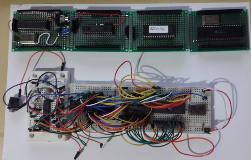
The blocks in the photo makes up a small 6502 system. It's the equivalent of the circuit on breadboard underneath it. The magic is the long pin female headers so that they can be stacked on top of each other. I brought all of the 6502's pins to the female headers. Chip select signals for each layer is routed through headers on the left.
From left to right,
- a swinsid (hardware that emulates c64's sound chip sid)
- 32k sram
- 32k eprom (of which I use only 256 bytes or so)
- 6502 itself
You can see it in action briefly here at the start of this video : https://www.youtube.com/watch?v=wW5FI8Fg1Jc
By the way, I tried to do the same thing to use TMS9918 but that one failed because I need to put 3 latches and also SRAM chip on the same layer which defeats the purpose of this stacking.
ps: For reference, here is an example long female header : http://www.aliexpress.com/item/100PCS-2 ... 14708.html
@ArnoldLayne :
Thanks for the info, I'll dig it up when I find time to switch back to the TMS9918 project. I need to do some soldering stuff for my prototype board before I can continue.
http://www.commodore.gen.tr/forum/index ... pic=9562.0
The blocks in the photo makes up a small 6502 system. It's the equivalent of the circuit on breadboard underneath it. The magic is the long pin female headers so that they can be stacked on top of each other. I brought all of the 6502's pins to the female headers. Chip select signals for each layer is routed through headers on the left.
From left to right,
- a swinsid (hardware that emulates c64's sound chip sid)
- 32k sram
- 32k eprom (of which I use only 256 bytes or so)
- 6502 itself
You can see it in action briefly here at the start of this video : https://www.youtube.com/watch?v=wW5FI8Fg1Jc
By the way, I tried to do the same thing to use TMS9918 but that one failed because I need to put 3 latches and also SRAM chip on the same layer which defeats the purpose of this stacking.
ps: For reference, here is an example long female header : http://www.aliexpress.com/item/100PCS-2 ... 14708.html
@ArnoldLayne :
Thanks for the info, I'll dig it up when I find time to switch back to the TMS9918 project. I need to do some soldering stuff for my prototype board before I can continue.
Re: Interfacing stock 6502 to TMS9918
@i_r_on:
Awesome. Yeah, like I said...we had the same idea. I've thought about building something similar. I thought about even having a PCB made for such modules. Shouldn't be too expensive.
If anyone has more TMS documentation then please let me know. I'd like to add it to my collection.
https://github.com/cbmeeks/TMS9918
Thanks
Cat; the other white meat.
Re: Interfacing stock 6502 to TMS9918
Hi all. This is a really interesting thread. I have been intrigued to know that there has been success in interfacing the 6502 @ 4Mhz to the TMS without any obivous problems. Currently my machine is running @ 2.7Mhz - the limiting factor is my AMD6551 ACIA. I have a WDC 6551 which will run at higher clock speeds, but will need to update my software to work around the serial bug. So for the moment will stay @ 2.7Mhz.
However, I have documented some of my video interfacing in the following log:
https://hackaday.io/project/5789-6502-h ... deo-output
Hope that helps.
Cheers.
However, I have documented some of my video interfacing in the following log:
https://hackaday.io/project/5789-6502-h ... deo-output
Hope that helps.
Cheers.