6502.org Forum  Projects  Code  Documents  Tools  Forum
It is currently Fri Sep 20, 2024 9:26 am

All times are UTC


Post new topic Reply to topic  [ 153 posts ]  Go to page Previous  1, 2, 3, 4, 5, 6 ... 11  Next
Author Message
PostPosted: Sat Dec 05, 2015 6:04 am 
Offline
User avatar

Joined: Fri Dec 11, 2009 3:50 pm
Posts: 3367
Location: Ontario, Canada
GARTHWILSON wrote:
Actually (as BDD likes to point out) you can get away with a slightly slower access time if you let the RAM chip select go true before phase 2 rises, and only use phase 2 to enable the WR\ or OE\
Hi, Garth. No big deal, but I'd like to zoom in on this for a moment. BDD's approach, which is also my own, often requires no extra gates. Would you agree that, as a zero-cost option, any benefit, even a small benefit, makes it an automatic win?

GARTHWILSON wrote:
RAM is available in faster speeds than anything else you're likely to use anyway, so it probably won't be the pacing item in terms of speed.
True, as far as it goes. But you seem to be saying, "Begin by checking what the timing specs indicate, and if the answer is satisfactory then forget further improvements." In my opinion it's better to say, "Begin by checking whether we can activate CS early for free."

I just think it's good engineering to shoot for the Inherently Superior approach first, as a default policy, and if necessary downgrade to Perfectly Satisfactory only as a secondary option -- yes, even though Perfectly Satisfactory may be perfectly satisfactory :roll: (according to published specs)!

Extra timing margin won't hurt, and may help -- especially when running the gear faster than published specs. :!: If there's any "upside" to discarding that extra margin then could you please explain?


BigDumbDinosaur wrote:
you have to be constantly aware of the use of the data bus to emit the bank address, which occurs when !Ø2 && (VDA || VPA) is true.
Do you have a reference for that, BDD? I've always assumed the bank address appears anytime Ø2 is low. Table 5-7 in the '816 datasheet tends to support that, as it lists a 24-bit address even for cycles when VPA=VDA=0.

Good point about bus contention. To get to the bottom of that we need to know if there's a transceiver (eg '245) on the data bus between the CPU and memory. If so, it probably floats during Ø2 low -- which changes the picture (for the better).

-- Jeff

_________________
In 1988 my 65C02 got six new registers and 44 new full-speed instructions!
https://laughtonelectronics.com/Arcana/ ... mmary.html


Top
 Profile  
Reply with quote  
PostPosted: Sat Dec 05, 2015 7:10 am 
Offline
User avatar

Joined: Fri Aug 30, 2002 1:09 am
Posts: 8510
Location: Southern California
Dr Jefyll wrote:
often requires no extra gates

Beyond the address decoding, you do have to add this, right?
Image
So it's probably not free (unless it's in programmable logic). As for trying to get extra setup time for the RAM though, tADS becomes almost the entire phase-2-low time as the processor approaches its maximum speed (according to the questionable data sheet), so "doing it right" does not bring any advantage unless the RAM is really slow and it's running out of gas while the processor still has considerable margin. For my SRAM module nowadays, I'm buying 512KB 10ns SRAMs for 1/16th what I paid for my first 8KB 120ns SRAMs in 1985 from Jameco. Adjusted for inflation, I paid over two thousand times as much per bit as I'm paying today, even though today's is 12 times as fast.

I was forgetting earlier that he was talking not about the '02, but about the '816 which puts the bank address on the data bus during the phase-2-low time. It shouldn't cause any contention though, as the '245 is disabled during this time.

_________________
http://WilsonMinesCo.com/ lots of 6502 resources
The "second front page" is http://wilsonminesco.com/links.html .
What's an additional VIA among friends, anyhow?


Top
 Profile  
Reply with quote  
PostPosted: Sat Dec 05, 2015 7:03 pm 
Offline
User avatar

Joined: Thu May 28, 2009 9:46 pm
Posts: 8389
Location: Midwestern USA
Dr Jefyll wrote:
BigDumbDinosaur wrote:
you have to be constantly aware of the use of the data bus to emit the bank address, which occurs when !Ø2 && (VDA || VPA) is true.
Do you have a reference for that, BDD? I've always assumed the bank address appears anytime Ø2 is low. Table 5-7 in the '816 datasheet tends to support that, as it lists a 24-bit address even for cycles when VPA=VDA=0.

Actually, that is true. :D I was including the state of VDA and VPA to subtly (or not-so-subtly) hint that they should be considered in any address decoding logic.

Quote:
Good point about bus contention. To get to the bottom of that we need to know if there's a transceiver (eg '245) on the data bus between the CPU and memory. If so, it probably floats during Ø2 low -- which changes the picture (for the better).

Although I haven't investigated it, it seems to me that a bus transceiver on D0-D7 is only necessary if loading dictates that more drive be made available. If used, then it can be gated so that isolates both sides of D0-D7 when Ø2 is low.

The reason I am surmising that is that 65xx peripherals do not emit data during a read cycle until tCDR nanoseconds after the rise of Ø2. Hence they will not cause bus contention with the 65C816 during Ø2 low. Non-65xx devices can have their /OE and /WE inputs gated by Ø2, which again deals with the bus contention issue.

Attachment:
File comment: Non-65xx Read/Write Qualification
read_write_qualify.gif
read_write_qualify.gif [ 32.21 KiB | Viewed 880 times ]

————————————————————————————
EDIT: Fixed improper data sheet reference.

_________________
x86?  We ain't got no x86.  We don't NEED no stinking x86!


Last edited by BigDumbDinosaur on Sat Dec 05, 2015 7:26 pm, edited 1 time in total.

Top
 Profile  
Reply with quote  
PostPosted: Sat Dec 05, 2015 7:08 pm 
Offline
User avatar

Joined: Fri Dec 11, 2009 3:50 pm
Posts: 3367
Location: Ontario, Canada
Good points, Garth. And let me say your viewpoint and mine don't differ widely -- I'm just clarifying. We have two questions.

  1. Are there cases where the early CS is free, and
  2. In a case where early CS is free then should you go that route -- especially when running the gear faster than published specs

Answer #1 is yes (example: with programmable logic). IMO answer #2 is also yes, remembering the premise that the extra access time is free. When a system is pushed to its limit and crashes, it's next to impossible to say that extra access time would help or wouldn't help. Certainly the questionable data sheet won't tell us.

GARTHWILSON wrote:
RAM is available in faster speeds than anything else you're likely to use anyway
I love how fast RAM's have become widely available! But not everyone uses them -- and ROM's (which can also benefit from early CS) are considerably slower.

GARTHWILSON wrote:
Beyond the address decoding, you do have to add this, right?
Good point. The little logic network you posted can be eliminated in some cases if we're willing to sacrifice the early CS -- I hadn't thought of that. It means cases of "free" early CS are less common than I thought (but the questions as stated remain valid).

FWIW, sometimes the little logic network is free. A ROM doesn't require /WR, only /OE, and the latter can be driven from /Ø2 if you have it (or just use PHI1O). Another case where the little logic network is "free" (no extra cost) is systems that use non-65xx peripherals -- they're gonna require /RD and /WR anyway. (Hmm, alright, I guess there are tiny costs. Example- running the PCB traces... )

-- Jeff

_________________
In 1988 my 65C02 got six new registers and 44 new full-speed instructions!
https://laughtonelectronics.com/Arcana/ ... mmary.html


Top
 Profile  
Reply with quote  
PostPosted: Sat Dec 05, 2015 7:15 pm 
Offline
User avatar

Joined: Fri Dec 11, 2009 3:50 pm
Posts: 3367
Location: Ontario, Canada
BigDumbDinosaur wrote:
65xx peripherals do not emit data during a read cycle until tDCW nanoseconds before the fall of Ø2.
tDCW is a spec associated with write timing. Do you mean tCDR? That is measured from the rise of Ø2.

I agree a bus transceiver on D0-D7 may be dispensible in some cases.

_________________
In 1988 my 65C02 got six new registers and 44 new full-speed instructions!
https://laughtonelectronics.com/Arcana/ ... mmary.html


Top
 Profile  
Reply with quote  
PostPosted: Sat Dec 05, 2015 7:23 pm 
Offline
User avatar

Joined: Thu May 28, 2009 9:46 pm
Posts: 8389
Location: Midwestern USA
Dr Jefyll wrote:
BigDumbDinosaur wrote:
65xx peripherals do not emit data during a read cycle until tDCW nanoseconds before the fall of Ø2.
tDCW is a spec associated with write timing. Do you mean tCDR? That is measured from the rise of Ø2.

Oops! :oops: I misread the data sheet. tCDR is correct and yes, it is measured as you describe. I had that part of the data sheet magnified and must've inadvertently scrolled up. :oops: It doesn't help any that I am (again) having vision troubles that were supposedly corrected via surgery two years ago. :(

Quote:
I agree bus a transceiver on D0-D7 may be dispensible in some cases.

One of the nagging little things about the '816 data sheet is that it doesn't explicitly state how much drive the '816 can produce on the buses. It would be nice to know that in terms of milliamps of source and sink. Garth seems to think that it's pretty substantial, but I have to wonder.

_________________
x86?  We ain't got no x86.  We don't NEED no stinking x86!


Top
 Profile  
Reply with quote  
PostPosted: Sat Dec 05, 2015 7:31 pm 
Offline
User avatar

Joined: Fri Dec 11, 2009 3:50 pm
Posts: 3367
Location: Ontario, Canada
BigDumbDinosaur wrote:
One of the nagging little things about the '816 data sheet is that it doesn't explicitly state how much drive the '816 can produce on the buses. It would be nice to know that in terms of milliamps of source and sink. Garth seems to think that it's pretty substantial, but I have to wonder.
The '816 datasheet has a long list of nagging little things not explicitly stated! :P :roll:

Why do you wonder about the drive current?

_________________
In 1988 my 65C02 got six new registers and 44 new full-speed instructions!
https://laughtonelectronics.com/Arcana/ ... mmary.html


Top
 Profile  
Reply with quote  
PostPosted: Sat Dec 05, 2015 7:34 pm 
Offline
User avatar

Joined: Thu May 28, 2009 9:46 pm
Posts: 8389
Location: Midwestern USA
Dr Jefyll wrote:
GARTHWILSON wrote:
RAM is available in faster speeds than anything else you're likely to use anyway

I love how fast RAM's have become widely available! But not everyone uses them -- and ROM's (which can also benefit from early CS) are considerably slower.

The fastest ROMs I've encountered to date are Atmel's 27C256 OTPs, which are rated at 45ns. POC V1.1 is stable at 14 MHz using this device.

I've been using AMD's 27C256 EPROMs ever since I started the POC project. At 55ns, they appear to be the fastest EPROMs currently available. The machine will usually boot at 14 MHz with this device, but can't be called stable. After all, at 14 MHz I am violating the EPROM's timing. :twisted:

_________________
x86?  We ain't got no x86.  We don't NEED no stinking x86!


Top
 Profile  
Reply with quote  
PostPosted: Sat Dec 05, 2015 8:01 pm 
Offline
User avatar

Joined: Thu May 28, 2009 9:46 pm
Posts: 8389
Location: Midwestern USA
Dr Jefyll wrote:
BigDumbDinosaur wrote:
One of the nagging little things about the '816 data sheet is that it doesn't explicitly state how much drive the '816 can produce on the buses. It would be nice to know that in terms of milliamps of source and sink. Garth seems to think that it's pretty substantial, but I have to wonder.

The '816 datasheet has a long list of nagging little things not explicitly stated! :P :roll:

Tell me about it! :shock:

Quote:
Why do you wonder about the drive current?

It implies the MPU's maximum fanout, which would be useful to know as one scales up one's design, even in a 100 percent CMOS system. For example...

When I added the SCSI host adapter (HBA) to POC V1.0, I had to reduce Ø2 from 12.5 MHz to 10 MHz, as the unit was not stable at the higher clock rate. Investigation showed that the presence of the HBA was dragging down the bus signals' amplitude, which I surmised was due to the extra parasitic capacitance caused by the HBA taking the buses off-board.

POC V1.1, which was basically a "reissue" of POC V1.0 with hardware patches rolled in and circuitry added to support the HBA's DMA channel, runs faster due to some better layout that shortened some circuit paths. Helping matters is that when I finally figured out how to use the SCSI DMA channel I redesigned the HBA's PCB, and again shortened some circuit paths, especially D0-D7. Also, it was around that time that I replaced the 53C94 SCSI ASIC with the faster and more technically advanced 53CF94.

The cumulative effect of these changes was that I could bump Ø2 back up to 12.5 MHz and achieve 100 percent stable operation. There's no question in my mind (such as it is) that the changes to the PCBs' layout reduced parasitic capacitance, contributing to the reclamation of the higher Ø2 rate. The gain in using the 53CF94 was mostly in code efficiency, as the MPU was spending less time in a busy loop waiting for the 'CF94 to emit or accept data during DMA channel transfers. As both the 53C94 and 53CF94 have the same input capacitance rating (10 pF), switching from one to the other theoretically had no effect on bus loading.

_________________
x86?  We ain't got no x86.  We don't NEED no stinking x86!


Top
 Profile  
Reply with quote  
PostPosted: Sat Dec 05, 2015 8:25 pm 
Offline
User avatar

Joined: Fri Dec 11, 2009 3:50 pm
Posts: 3367
Location: Ontario, Canada
So you wonder about Garth's estimation of the drive current because the slowdown and reduced amplitude you observed seems excessive?

BigDumbDinosaur wrote:
Garth seems to think that it's pretty substantial, but I have to wonder.

_________________
In 1988 my 65C02 got six new registers and 44 new full-speed instructions!
https://laughtonelectronics.com/Arcana/ ... mmary.html


Top
 Profile  
Reply with quote  
PostPosted: Sun Dec 06, 2015 6:49 am 
Offline
User avatar

Joined: Thu May 28, 2009 9:46 pm
Posts: 8389
Location: Midwestern USA
Dr Jefyll wrote:
So you wonder about Garth's estimation of the drive current because the slowdown and reduced amplitude you observed seems excessive?

I think Garth's idea of how hard the '816 drives the buses is based on what he has observed with the 65C22. However, what I observed doesn't suggest the strong drive that Garth's believes is present.

_________________
x86?  We ain't got no x86.  We don't NEED no stinking x86!


Top
 Profile  
Reply with quote  
PostPosted: Thu Dec 10, 2015 6:29 pm 
Offline

Joined: Mon Oct 12, 2015 5:19 pm
Posts: 255
Whoa! Alot of comment since my last post. I have been trying hard to do my homework before I come and post "silly-reflections" and speculations. I will read your postings (since 12/4) and respond.

I have reached a few new conclusions. I think I need a multilayer board. I don't want to "farm out the work" as that is "cheating"; I was thinking maybe I could make my own multilayer board (but couldn't find a source for pre-peg; and, anyway, not sure I have the oven to get it "cooked" properly).

So I thought, maybe, two double sided boards with a "peg board" (unclad) between them. Inward facing boards could be power and ground planes, and the pegboard separates those two. Total stack would be 1/16" *3 = approx. 5 mm. The DIP pins should extend through that (though I didn't check the schematics yet). The boards could be held together by , say, five nuts and bolts; the copper around each nut and bolt should be etched, so no contact is made with the circuits.

Maybe you fellas know of some kind of glue, for inbetween the boards? I dunno, just a thought. I am going to proceed with a four-layer design and a two-layer design.

I'll be using PhotoEZ sheets for the silkscreen pattern; but I see some stuff on the internet for laser print/toner transfer techniques. Maybe I'll try that someday, but I know PhotoEZ works (its just a bit expensive, I think).

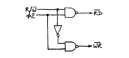
Also, VIAs; I was reading Garth's primer and saw that his decoding scheme allowed for about ten of them. The decoding circuit that I presently have is wholly inappropriate. I leave 16KB (Kilo-locations) for I/O. Is there any GOOD reason to do this?

I am reworking "the plan" as we speak.

Thanks, again. I will read and comment later on the above discussions (also, I am still confusing myself over the "RAM-decode+clock" advice of Garth's; But I will have it worked out very soon ( viewtopic.php?f=12&t=3539 ). Timing diagrams, I am sure, are tricky. I just haven't had the "mental fortitude" to tackle it, just yet.

On the plus side, my parts situation is shaping up nicely. All the more reason for me to "finalize" some kind of design.

It would be awesome if I could work the Kodak image sensor project into the 6502 project. Still studying I2C and 65C22 to get a handle on how this REALLY works.

Any advice on running 65816 and 6522 at 3.3V, so that the Kodak sensor device matches (Kodak sensors CANNOT be 5V!). I don't mind buying a new EEPROM and RAM, but I am not sure I could find ones that run at 3.3V?

Maybe 5V computer is what I should stick with, and try to alter the Kodak signal to interface with the 6522? Any tips for that sort of a plan? (I should read all of my posts since joining two months ago; who was it that warned me against "flying a jumbo jet; before piper plane"? Smart person, whoever it was!). Cheers.

(P.S. I watched a youtube video about Nolan Bushnell, Atari founder, yesterday. His original plan was to take a small cheap microcomputer and hook it up to 6, then, 5, then 4 displays, and amortize the cost of the computer, by having kids pump it full of quarters. At 3 video screens the cost made no sense, so he abandoned the project when he couldn't keep up with the I/O. He moved to "hardwired", "many-chip", state-machines, for creating the video arcade market (though pinball already existed, I guess); not full von-Nuemann, because of this. He also mentions an interesting anecdote about "keeping all the NMOS fabs under his employ, to guarantee his near-monopoly on the gaming market". It worked for awhile.)


Top
 Profile  
Reply with quote  
PostPosted: Thu Dec 10, 2015 6:49 pm 
Offline

Joined: Mon Oct 12, 2015 5:19 pm
Posts: 255
Garth, especially, Thank you a million for your always detailed an patient instruction. I kow alot of this stuff, and can tell when I am getting good advice; but I am a bit "out in the sticks" of Vermont, and don't have alot of experts to double check me. Your help is invaluable, and I am not "just saying that". (you other guys too!Thanks, really...).

Quote:
"If you want to just always be in the practice of doing it the best it can be without incurring extra cost, go for it. It may pay off nicely later.~Garth"


Yes, quite important to do things right. I don't know what is possible with digital systems, but I intend to push any and all limits that will accomplish my goal (i.e. Strong AI, based upon my "simplified/simplistic-human-language-algorithm"). Vision is task one. Audio, mostly accompished by a hundred years of excellent American music--abd more prcisely, the endeavour to capture said music, electronically--is the next task, with touch, smell, and taste folllowing. then what to do with the sense information, once it is all in one place! Aha! There's the rub!

You're right. I was not describing a ground plane (or micro-strip or anything like that!). But NOW I am (my latest PCB patterns, both 2 and 4 sided, are incorporating ground planes) describing ground planes. I don't follow the traces entirely, but for most of their length.

The "two side" board is maybe a fantasy. i don't know. I do have my "plated thru hole" stuff, and was thinking about maybe even trying to do that. If I do the four-sided board--my DIY method-- I might plate-thru-holes both double sided boards and then try to fasten them together and to the empty-pegboard. I am still fluid on methodology; nothing set in stone just yet. If I think I can accomplish everything on a two sided board, then I will; for cost and simplicity reasons.

Hey Garth, does anybody sell a ten-VIA board; pluggable like your SRAM board?

OK, I gotta go (time-share computer! Thought they went out of stkle in the 80s!!! hahaha!) Cheers.


Top
 Profile  
Reply with quote  
PostPosted: Thu Dec 10, 2015 6:57 pm 
Offline

Joined: Mon Oct 12, 2015 5:19 pm
Posts: 255
Whoops; thanks for catching that. Must cogitate ....

Quote:
"The memory module is 4Mx8, which is 4 megabytes, or 32 megabits. It is not 32 megabytes. It has up to eight 512kbyte ICs, which are the most I've seen for 5V. There have been two customers that have ordered four boards at once, in order to get 16MB (128Mb)."


Quote:
"For the W65C22N, the input high voltage is a minimum of 2.0V, whereas for the W65C22S, it's much higher, 3.5 or 4.0 for a 5V power supply, depending on what part of the data sheet you believe. (Yeah, WDC's data sheets have problems!)"


Thanks for the "heads up"; I will read this advice a couple more times and keep thinking about it while I look at I2C and 6522s (I mean W65C22S and W65C22N) ... I really have to get in the habit of using the right part number and not being so "informal".

I think, since I will be home on my "air gap computer" I will do a bit of work on the decoding schematic; labelling pins and such; so that I might speak intelligently about the evolution of my PCB design. Maybe tomorrow or next day, something "bright" will be posted, by me.


Top
 Profile  
Reply with quote  
PostPosted: Thu Dec 10, 2015 7:04 pm 
Offline

Joined: Mon Oct 12, 2015 5:19 pm
Posts: 255
Quote:
"If your RAM or ROM has its /OE permanently tied low and the '816 is in a read cycle (RWB is high ... ~BDD "


Hey thanks. As I stated above, I am out "in the sticks" with little valid conversation on this particular subject. My "Newbie-ish-ness" is taken for expertise among my friends, and it seems that only I know enough about the subject to understand how WRONG that is!

Thanks for looking at it. But, I HAVE TO DO MY HOMEWORK. I put it off too long. I have some of the schematics up on this thread, already, but I should zoom in, post a few pictures of the detailed areas of concern, and ask REAL, RELEVANT questions.

Suffice it to say, my OE/ pins and my decode circuit must change; and my attention to timing diagrams must become obsessive!


Top
 Profile  
Reply with quote  
Display posts from previous:  Sort by  
Post new topic Reply to topic  [ 153 posts ]  Go to page Previous  1, 2, 3, 4, 5, 6 ... 11  Next

All times are UTC


Who is online

Users browsing this forum: No registered users and 47 guests


You cannot post new topics in this forum
You cannot reply to topics in this forum
You cannot edit your posts in this forum
You cannot delete your posts in this forum
You cannot post attachments in this forum

Search for:
Jump to: