Hi all
Here's an update with my 65C02v2 project. This is the one with the bank switching.
So far, so good. The board reads and executes instructions from ROM fine and can read/write bank 0 RAM. I've (literally) just now soldered in the links for the bank switching latch to the RAM and the decoding GALs. Should hopefully be able to do some tests tomorrow.
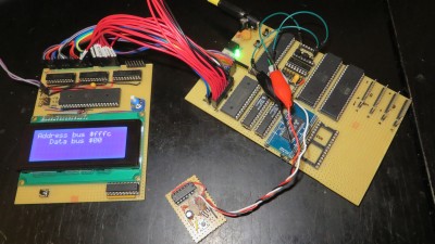
I'm especially happy with the RAM as it supports both the AS6C1008 and AS7C1024B (using an adapter). Both have the same pin-out and are 128KB (1Mbit). The main difference is that the AS6C1008 is a DIP package and is spec'd at 55ns while AS67C1024B is a SOJ32 and is spec'd at 10ns.
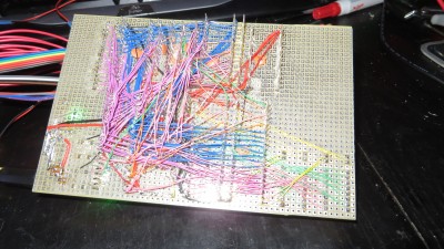
Here's a coupe of pictures (with AS7C1024B). The board has been tested fine at 25MHz divided down to 12.5MHz (via a D type flip flop). Haven't got anything faster crystal oscillator-wise at the moment, but I've got some on order (40MHz and 50MHz - so tests will be at 20 and 25MHz respectively).
Still need with hook up the VIA and ACIA IRQ lines.
The NMI is hooked up to a DS1813 power monitor and push button combo. I plan (as suggested by forum members) to have this as a "get out of jail free" option in case the computer locks up in a loop. I don't have the code for this at the moment, but I'll sort that out later.
Attachment:
 65C02v2.JPG [ 1.45 MiB | Viewed 719 times ]
Attachment:
 65C02v2_u.JPG [ 1.98 MiB | Viewed 719 times ]


